Thermal methods such as differential scanning calorimetry (DSC) and thermo mechanical analysis (TMA) are well-established techniques for characterizing polymers, thin films, and coatings. However, DSC requires a sample mass of 5 mg or greater for accurate results to be obtained. Smaller sample masses can be analyzed with DSC, but extreme care must be taken not to induce thermal or mechanical stresses into these during the sample preparation. When the total mass of sample used in a particular application is less than 500 µg, there are few options left to the materials analyst. One option is to extract multiple samples and accumulate sufficient mass to generate a reasonable instrument response; however, this option is rapidly losing favor with device manufacturers in optical telecommunications/medical devices, where the cost of these devices rises into the hundreds or even thousands of dollars per sample.
A second option for determining the cure state or glass transition temperature (Tg) of an adhesive is the use of thermal mechanical analysis. This technique uses a quartz probe with a diameter that ranges from 0.5 mm to 4 mm or greater to measure the expansion of a material as a function of temperature. With TMA, the issue becomes one of sample size, and when the sample is 1 mm or less, the TMA option reaches its practical limit.
This limitation of conventional thermal methods makes them unsuitable for the following rapidly growing application classes:
- Samples with minimal amounts of material. These include applications such as ultrathin films/coatings and measurements of micron-scale devices such as those used in optical telecommunications and medical devices.
- High-spatial-resolution thermal property mapping. This is used to identify local defects, characterize thermal property gradients, or more generally correlate spatial heterogeneity to thermal property information.
- Time-resolved thermal property studies. These include applications in which measurements are taken over time to watch the evolution of thermal properties on the same sample, for example, studies on cross-link density formation/cure rates of a film or coating.
The techniques of nano-thermal analysis (nano-TA) and transition temperature microscopy (TTM), on the other hand, are perfectly adapted to solve these important application classes. They are discussed in more detail below.
Description of nano-TA and TTM
 Figure 1 - Illustration of nano-TA and TTM techniques.
Figure 1 shows the principle of nano-TA and TTM. The nano-TA technique uses a nanoscale thermal probe to locally heat the surface of a sample while simultaneously monitoring the softening of the sample surface under the heated probe.1–6 As shown, the nano-TA measurement is a plot of probe deflection versus probe tip temperature while the temperature is ramped with the probe tip in contact with a region of a sample. The probe initially deflects upward due to the thermal expansion of the sample. Events such as melting or glass transitions that result in the softening of the material beneath the tip produce a downward deflection of the cantilever or a change in slope of the deflection versus temperature curve.
TTM extends the nano-TA technique into an imaging or microscopy mode by assembling an array of nano-TA measurements into an image or map of the transition temperatures across the region of interest. In TTM mode, the probe is translated automatically over the sample, and the nano-TA procedure is repeated for the array of points over the user-defined XY region of interest. The array of nano-TA measurements is automatically analyzed to determine the transition temperature at each point or pixel within the scanned region. Then, a false color map is created where the pixels are shaded according to the measured transition temperatures. The resulting spatial map allows visualization of thermal gradients and can detect the presence of inhomogeneities in a wide range of samples. The TTM image can also be analyzed by plotting the transition temperature versus lateral position on the sample as well as selecting points from the image to generate a histogram of transition temperatures.
 Figure 2 - Scanning electron microscope (SEM) image of the microfabricated nanoscale thermal probe used for nano-TA measurements. The inset is a zoom of the tip that makes contact with the sample surface and that has a radius of <30 nm.
The nano-TA technique is analogous to bulk TMA, except that nano-TA characterizes the thermal response of a small amount of material in proximity with the probe tip and therefore can locally determine the transition temperature of the sample on the micro- or nanoscale. Similar to probes employed for atomic force microscopy (AFM), the nano-TA probe, shown in Figure 2, is made using microfabrication techniques allowing very small geometries and repeatable performance.7 The apex of the probe that contacts the sample surface has a radius that is less than 30 nm, and the probe incorporates an embedded miniature heater that permits localized heating. Because of its small size, the temperature of the probe can be changed quickly, enabling heating rates from 5 °C/min to 600,000 °C/min. This allows the measurement time per point to be faster than 1 sec, thus significantly improving throughput and permitting multiple measurements across a sample surface in a reasonable amount of time.
Applications enabled by TTM
The following section will describe application classes in which TTM was utilized, and show how the technique enables us to more fully characterize samples that are inherently challenging for regular thermal analysis techniques.
1. Thermal analysis of micron-scale applications such as photonic devices. The development of and subsequent miniaturization of photonic devices has resulted in new challenges for analytical scientists. Adhesives are frequently used in the fabrication of miniature photonic devices, and the curing process can have a dramatic effect on device performance. Determination and verification of an adhesive’s properties are absolutely critical to ensure the proper functioning of high-performance photonic devices. However, miniaturization has brought a large reduction in the mass of an adhesive used in a particular device. Whereas in the past one might be able to extract several milligrams of sample from a single device for analysis, current devices are using less than 0.1 mg. The reduction in adhesive mass also means less heat generated during the cure process, which can significantly alter the cure kinetics.
These challenges become especially important when materials are applied on scales far smaller than the scales available for characterization. The lack of scale-appropriate upstream characterization can require expensive downstream characterization and functional testing, often requiring the sacrifice of many devices to collect enough sample data. Issues in process variation can result in expensive yield loss and excess scrap. For photonic devices requiring high stability, variations in cure states of adhesives result in unacceptable levels of volatile compounds. This can contaminate the optical path and increase thermal expansion and moisture absorption, resulting in serious deterioration in performance. Optimal cure of the adhesives used in a photonic device is first and foremost in ensuring long-term performance. Verification of an epoxy’s cure state in a functional device is the first step in ensuring long-term performance and survivability. It is generally assumed that a uniform cure state exists in a UV or thermally cured adhesive; however, this is largely a function of the sampling dimensions and not the true material state. Thermal gradients as well as shadowing in UV-cured adhesives greatly affect the final cure state of adhesives, and proof of a manufacturing protocol is very important.
 Figure 3 - a) Epoxy-coated annulus of an
optical encoder that was measured using
nano-TA. Red “+” indicates the approximate
locations of the measurements. b) nano-TA
measurement at the center of the annulus
on sample A. c) nano-TA measurement at
the center of the annulus on sample B.Figure 3 shows an optical encoder whose epoxy was analyzed using nano-TA. Data from nano-TA were taken on two similar optical encoder devices, sample A and sample B, that were manufactured using the same epoxy but cured at different temperatures (105 °C for sample A and 120 °C for sample B). At each location, two measurements were taken to characterize the curing of the epoxy caused by the first temperature ramp.
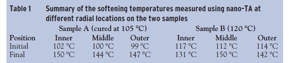
Data were taken at three different locations (Figure 3a) on the epoxy annulus for both sample A and sample B. Figure 3b and 3c show the data for the center of the annulus for sample A and sample B, respectively. The data suggest different undercured states in both devices, varying with radial location on the device surface. The results are summarized in Table 1, which suggests the lowest cured regions to be on the outermost diameter of the annulus.
The nano-TA technique allowed for the characterization of a single thin adhesive film of less than 10 µm thick, across a surface less than 3 mm in diam. The test data for this device clearly show an effect of cure temperature as well as a gradient in the Tg across the device. More importantly, the data show a large change in the Tg after the first heating of the sample. The 105 °C cured adhesive has an initial Tg range of 99 °C to 102 °C and a second heat Tg range of 144 °C to 150 °C. For the 120 °C cured adhesive, the initial Tg range is 112 °C to 117 °C, while the final Tg range is 131 °C to 150 °C. (Note: the ultimate Tg for this adhesive is 155 °C.)
The significance of the increase in Tg as shown in the second heat is that it indicates that the adhesives were not adequately cured during the previous manufacturing cycles (105 °C and 120 °C). This finding is key to why the nano-TA technique is so valuable to any industry with expensive micron-scale samples. The technique was able to obtain multiple results on each individual sample, unlike traditional techniques like DSC, where one would need to use between 20 and 50 devices to have an adequate sample. The nano-TA technique is unique in its ability to determine submicron-scale thermal properties of adhesives and thermoplastics. In a manufacturing world in which small is truly becoming micro and perhaps even nano in scale, the ability to measure and confirm the properties of bonding agents is critical.
2. High-spatial-resolution thermal property mapping. Correlating thermal properties to spatial heterogeneity is useful for a broad range of samples, including analyzing uniformity within different layers in a multilayer film or a single layer as well as identifying defects. This is illustrated with the examples below.
a. Thermal property mapping of a multilayer liquid crystal display (LCD) film. The different layers in multilayer films are often engineered and designed to contribute to the final performance of the ensemble. However, no direct methods are currently available to study the thermal properties of the individual layers or interfaces once they are embedded in the composite stack. Transition temperature microscopy can solve this problem by providing a convenient method for spatially resolving the thermal response of individual layers and their interfaces by generating transition temperature maps of areas scanned by the thermal probe. Polymers are an integral part of flat panel displays and most often are applied as thin films in order to provide their functionality. The critical property of flat panel displays is clearly the optical dispersion characteristics of the materials that combine to control resolution, brightness, and contrast. Since light scattering is impacted by the density distribution within films, density variations associated with chemical and structural heterogeneities will play a dominant role in the measured refractive index and performance. Moreover, the temperature dependence of density makes thermal property measurement more significant for both the design of electronic displays and for failure analysis.
 Figure 4 - a) Optical image of a cross-sectioned multilayer LCD film showing the various layers. b) 80 × 200 µm TTM image of the cross-section shown in (a), which is positioned so that the features are aligned with the corresponding optical image in (a). c) Histogram of the transition temperatures in the TTM image allowing measurement of the average and distribution of transition temperatures in the various layers.
A polymer multilayer from an LCD was microtomed in order to gain access to the different layers within the LCD stack, and the cut surface was then imaged using TTM. Figure 4a shows an optical image that reveals the multiple layer construction of the LCD stack; the layers range in size from a few microns to many tens of microns. Figure 4b is the corresponding color-coded TTM image that is scaled to track with the optical image. This figure clearly illustrates the variation in thermal properties across the different layers that are not evident in optical micrographs.
TTM can also detect the presence of thermal gradients and thermal transitions within layers. In addition, TTM images can provide a quantitative measure of the spatial distribution of thermal inhomogeneities in the form of thermal property maps. Such features are usually not visible or detectable in optical images. Transition temperatures can also be displayed in the form of a histogram, which provides a plot of the measured distribution of thermal (and hence mechanical) properties over the sample. This superposition of thermal analysis and microscopy makes TTM unique in its ability to generate high-resolution thermal property maps.
b. Analysis of blown polyolefin thin films. TTM provides a new analytical capability to determine the cause of variations between different homogeneous thin films. Blown polyolefin thin films are utilized in a broad range of packaging applications. In this example, the films were used to form an ice bag. Two different films that were processed in the same manner had different performance, with one of the polyolefin films failing early and causing breakage of the bag. A number of bulk thermal analysis techniques were performed on the films to try to determine the cause of the early failure. Some of the bulk techniques could differentiate between the two different films, but they did not lead to an understanding of the source of the difference.
 Figure 5 - TTM images (bottom) of a “good” (c) and “bad” (d) film and histograms (top) of the calculated transition temperatures for each image. The histograms show the higher transition temperature and larger variation in the “bad” film.
TTM was then used to analyze various locations on the surface of the two films. Figure 5 shows the results from TTM measurements that were taken over a 200 × 200 µm area on the “good” film (Figure 5c), and a 100 × 100 µm area on the bad film (Figure 5d). As can be seen from the histogram from each image, the bad film had a higher onset of melt temperature with significantly more variability in the local transition temperature. This variability in transition temperature is probably due to inhomogeneous crystallinity, which may be the source of local stress sites in the film. These stress sites may be the cause of the early failure. The ability of TTM to spatially resolve variations in crystallinity within the polyolefin thin film added significantly to the understanding of the failure mechanism with this film.
c. Time-resolved cure-rate measurements in auto refinish coatings. Automotive refinish clearcoats are cross-linked coatings that are usually cured through a reaction between two or more components. The primary function of clearcoats is to protect themselves and the coatings under them against environmental influences and provide scratch, mar, and chip resistance, as well as erosion and solvent resistance, while still maintaining a high gloss and excellent appearance.8 Due to the fact that the clearcoat is the first line of defense against environmental influences, understanding surface, near-surface chemical, and mechanical property development as a function of composition, cure time, and environmental exposure is fundamental to improving their performance. Furthermore, the demand for lower volatile organic carbon (VOC) systems in the automotive refinishing industry means that new resins, solvents, and additives are being introduced. This, coupled with demands for attaining fast cure at ambient temperature in order to reduce the investment in drying equipment and the time for repair, points to the need for a thorough understanding of the dynamics of film formation.
 Figure 6 - nano-TA measurements of a clearcoat measured at three different times after deposition (a) and the plot of softening temperature versus cure time (b).
Figure 6 demonstrates how nano-TA can be used to follow the cure kinetics that take place at the coating surface. Figure 6a displays the temperature ramps taken on an acrylic clearcoat at three different times after the coating was deposited. The softening temperature can be easily measured from these curves and, if plotted versus cure times (Figure 6b), provides critical information on cross-linking rates and reaction kinetics. The ability to measure chemical kinetics opens new avenues for exploring the effects of composition, additives, and processing conditions on the speed of film drying and mechanical property development at surfaces and interfaces. The ability to measure rates of chemical processes can also yield information about the reaction mechanism and transition states, and also provide mathematical models that can be used to quantify and describe the time scales of the chemical reactions.9
As can be seen in Figure 6a, the transition temperature (which is a direct function of the cross-link density) shows a linear correlation with cure time. Since the molecular structure and thermodynamics near the air–surface interface usually differ from the bulk, this can lead to significant deviations in glass transition temperatures and modulus as measured by methods such as DSC or TMA.10,11
Conclusion
Transition temperature microscopy is a technique that combines the benefits of microscopy with nanoscale thermal analysis. The addition of a probe with an integrated heater to an optical microscope or an AFM adds a new dimension and the valuable capability of spatially resolved thermal analysis. This combination facilitates the characterization of complex, heterogeneous, and multilayer structures by providing high-resolution thermal property mapping. The ability to heat and test very small regions of a sample surface enables the TTM technique to be valuable in applications ranging from in situ analysis of micron-scale devices to coating defect analysis and time-resolved dynamic measurements for coating design. The technique is made possible by the recent advances in microfabricated thermal probe technology, which permit scientists to heat and measure thermal properties from regions on the nano- and microscale.
References
- Zhou, J.N.; Douglas, J.F.; Karim, A.; Snyder, C.R.; Soles, C.L.; Berry, B. Nanoscale thermal and mechanical probe determination of softening transitions in thin polymer films. Nanotechnology2008, 19, 495703 (9 pp).
- Harding, L.; King, W.P.; Craig, D.Q.M.; Reading, M. Nanoscale imaging of partially amorphous materials using local thermomechanical analysis and heated tip pulsed force mode AFM. Pharm. Res. Nov 2007, 24(11), 2048–54.
- Nelson, B.A.; King, W.P. Thermal analysis with nanoscale spatial resolution using heated probe tips. Rev. Sci. Instr.2007, 78, 023702.
- Nelson, B.A.; King, W.P. Temperature calibration of heated silicon atomic force microscope cantilevers. Sensors and Actuators A Oct 2007, 140, 51–9.
- Germinario, L. Nano thermal analysis of polymers, thin films and coatings. Paper presented at Microscopy and Microanalysis Conference, Fort Lauderdale, FL, Aug 5, 2007.
- King, W.P.; Saxena, S.; Nelson, B.A.; Weeks, B.L.; Pitchimani, R. Nanoscale thermal analysis of an energetic material. NanoLett.2006, 6, 2145–9.
- King, W.P.; Kenny, W.T.; Goodson, K.E.; Gross, G.; Despont, M.; Dürig, U.; Rothuizen, H.; Binnig, G.K.; Vettiger, P. Atomic force microscope cantilevers for combined thermomechanical data writing and reading. Appl. Phys. Lett.2001, 78, 1300–2.
- Schmidt, E.V. Exterior Durability of Organic Coatings. FMJ Intern. Publishing: Redhill Surrex, 1988.
- Germinario, L.T.; Shang, P.P. J. Therm. Anal. Calorim.2008, 93(1), 207–11.
- Herminghaus, S.; Jacobs, K.; Seemann, R. Eur. Phys. J. E: Soft Matter2003, 12, 101–10.
- Forrest, J.A.; Dalnoki-Veress, K. The glass transition in thin polymer films. Advances in Colloid and Interface Sci.2001, 94, 167–97.
Mr. Kjoller is co-Founder and VP of Product Development, and Mr. Sahagian is Applications Engineer, Anasys Instruments Corp., 25 W. Anapamu, Ste. B., Santa Barbara, CA 93101, U.S.A.; tel: 805-730-3310; fax: 805-730-3300; e-mail: [email protected]. Mr. Rose is President, Rose Consulting, Half Moon Bay, CA. This article was partially excerpted from the poster entitled, “Transition Temperature Microscopy: A New Technique for Probing Nanoscale Thermal Properties of Polymeric Materials” (K. Kjoller, et al.), presented at the European Polymer Forum, Graz, Austria, July 12–16, 2009.