Helium ion microscopy (HIM) offers the highest spatial resolution surface imaging of any scanning beam method, as well as extremely high surface sensitivity. These factors combine to provide unmatched sample information at the nanoscale. Add to this the tool’s unique charge control technology, and several applications problems can be addressed. This article presents a sampling of recent results.
Biological imaging
A previous article1 in American Laboratory provided an introduction to the technology of the ORION™ helium ion microscope (Carl Zeiss SMT, Inc., Peabody, MA). There is much focus in current research on nanoscale dynamics in structural biology, pathology, and similar applications of microscopy. Many of the fundamental properties of biological systems are derived from behavior at this length scale. The makeup of such samples is largely hydrocarbons, once they are dried for microscopy. Gathering structural information at the nanometer length scale, then, requires the ability to image highly charging materials that are also of low weight and thus partially transparent to an electron beam. Both of these problems are traditionally handled by using a conductive coating on the sample, so that an SEM is actually imaging a thin metal shell over the sample. There is a downside to this, though, since every additional sample modification step can introduce artifacts and hide surface detail. For highly three-dimensional samples, it may be difficult to obtain a charge-free surface, even with coatings.
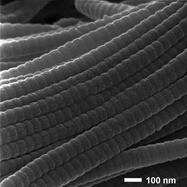
Figure 1 - HIM image of collagen fibers from the knee joint of a mouse. An Au-Pd coating had been applied. (Figure courtesy of Carl Zeiss SMT, Inc.)
Figure 1 gives an example of such a case. The image shows collagen fibers from the knee joint of a mouse, prepared by critical point drying (CPD) and coating with Au-Pd. It was not possible with SEM to achieve charge stability and thus good imaging, probably due to the inability to achieve uniform coating of the sample. Using the low-energy flood gun charge neutralization system in the ORION, however, it is straightforward to obtain stable contrast and thus sharp imaging. The banding in the fibers is extremely crisp, and the large depth of field provided by HIM gives a clear 3-D representation of the sample. Also note the unfortunate artifacts arising from the coating of this sample, which is manifested in the nanometer-range grains visible all over the surface. While showcasing the resolution capabilities of the tool very well, this false information is undesirable for sample analysis.
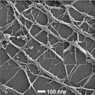
Figure 2 - Actin from a cytoskeleton after nucleus extraction and CPD. No conductive coating. Inset: magnified view of outlined filament. (Figure courtesy of Carl Zeiss SMT, Inc.)
An example of imaging uncoated samples is shown in Figure 2. In this case, the actin filaments of a cytoskeleton were being studied.2 A detergent process was used to remove the nucleus of the cell, and the sample was then prepared by CPD but not coated. High-resolution imaging of even the smallest actin filaments could be achieved. The inset of the picture shows a filament that is 7 nm at its narrowest, with an apparent helical structure.3 More work is necessary to verify the nature of what is being seen, but this proves the ability to measure such small features on uncoated samples.
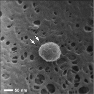
Figure 3 - Rat renal tissue with 100-nm nanoparticle. Uncoated sample, prepared by CPD. (Figure courtesy of Carl Zeiss SMT, Inc.)
As mentioned above, the coating process can obscure small sample features. Studies of the possible health effects of nanoparticle uptake in the body rely on accurate measurement of just such features. Figure 3 shows a dried but uncoated section of rat renal tissue from an animal that had been exposed to metal nanoparticles.2 HIM imaging was able in this case to see not only where the particles lodged in the tissue, but it also revealed hitherto undetected 5-nm pores in the tissue (arrows). Previous methods, requiring metal coating of the sample, covered these features.
Bioengineering
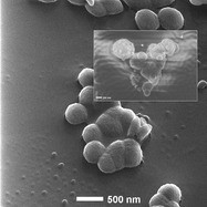
Figure 4 - Hydroxyapatite (presumed) crystals growing on a PLLA surface. HIM image. Inset: Scanning electron microscopy (SEM) image from a similar sample. (Figure courtesy of Carl Zeiss SMT, Inc.)
The biocompatibility of medical implants depends critically on the nature of the interface to the body. The material should promote cellular response in a manner similar to natural tissues. Thus, nanoscale structural characterization is warranted. The engineering of bone implants, for example, involves study of the earliest stages of mineralization of the implant surface. Figure 4 shows HIM imaging of a bioengineering polymer (PLLA) that had been immersed for 1 hr into a simulated body fluid. Previous SEM imaging (inset) suffered from shortcomings that prevented high-resolution characterization: Serious charging frustrated the imaging when no conductive coating was used. The contrast and surface detail were not obtained even when charge control measures were applied. A bigger hurdle in this case was the beam-induced damage to the initially flat polymer surface, which blocked any attempts to see the smallest growth. The charge control possible in HIM allowed high-resolution imaging with excellent surface detail. Due to the different nature of the beam–sample interaction, the polymer surface remains undisturbed, so that growths down to 50 nm could quickly be identified.
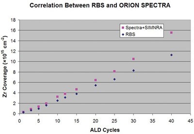
Figure 5 - Plot comparing thin film measurement data from RBS and HIM Spectra techniques on atomically thin films. (Figure courtesy of Carl Zeiss SMT, Inc.)
The very strong surface sensitivity of ion scattering spectroscopy (ISS) makes it an effective technology for analyses of surfaces and thin films. The energy of backscattered particles in techniques such as Rutherford backscattering spectrometry (RBS) or medium energy ion scattering (MEIS) can indicate film thickness and elemental composition. A drawback to these techniques is the large beam size—about 1 mm—and the need to carry out measurements at dedicated beam facilities. The relatively low-energy (30 keV) helium ion beam in the ORION can be used for these measurements due to the incorporation of a solid-state energy proportional detector. This Spectra™ option permits in-microscope measurements on small areas targeted in the HIM image. Figure 5 shows a direct comparison of RBS and Spectra analyses from a set of ultrathin films of ZrOx on silicon.4 There is good correlation between the film thickness in the two methods. The offset between the two data sets likely arises from a lack of low-energy cross-section data in the SIMNRA® analysis program (Max Planck Institute for Plasma Physics, Garching, Germany) used. Future efforts will address this issue. This technique now makes it possible to locate patterned thin film areas or small particles and carry out ISS with submicron spatial precision.
Patterning
HIM can be used to modify or even fabricate materials on the nanometer scale. There are two general approaches: lithography and beam-induced deposition. The former is based on chemical alteration of a soluble cover layer (a resist) on a substrate material. The resist changes its solubility when exposed to high-energy particles, e.g., electrons or helium ions. The differences in solubility are being exploited to remove only the beam-exposed areas, or, for the opposite application, to retain those areas.
A crucial test of any lithography technique is the resolution, i.e., minimal feature size possible. Another important issue is the disturbing effect that exposure in one area might have on the surrounding areas, the so-called proximity effect. A strong proximity effect would hinder lithographical production of dense and fine structures. For example, templates for molecular binding need dense structures with fine details.5
A 5-nm-thick hydrogen silsesquioxane (HSQ) resist layer on a silicon wafer substrate6 was exposed in the HIM. The tool was equipped with a pattern generator (Raith Elphy, Dortmund, Germany), allowing for exposure patterns of arbitrary shape. The authors wrote with the ORION lines as a single row of pixels at a mutual distance of 4 nm. Afterward, the exposed resist layer was developed.
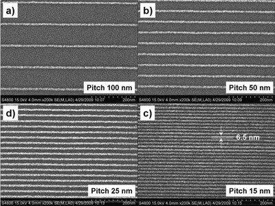
Figure 6 - Lines written with a subnanometer He+ beam in 5-nm-thick HSQ resist layer. Average line width is 6.5 ± 1 nm, independent of pitch. This result shows that small objects at high density can be made via helium ion beam lithography. (Figure courtesy of Carl Zeiss SMT, Inc.)
Figure 6 shows the result. Clearly, thin lines have been made in the resist. Their width is 6 ± 1 nm. Interestingly, the width and height of the lines do not depend on the pitch. Also, for the smallest pitch of 15 nm, all lines are well resolved. The lines are not affected by the neighboring lines. In other words, proximity effects are weak if not absent. This work shows that helium ion beam lithography provides the same resolution, or minimal feature size, as normal electron beam lithography, but without the proximity effects that plague the latter technique.
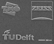
Figure 7 - Logos of the contributing parties, made by helium ion beam-induced deposition of Pt on silicon. The bright areas consist of platinum and carbon. The smallest gaps visible are only 12 nm wide. (Figure courtesy of Carl Zeiss SMT, Inc.)
The other nanofabrication approach is beam-induced deposition. In this case, the substrate is exposed to a precursor gas. An OmniGIS™ unit (Omniprobe, Inc., Dallas, TX) was fitted to deliver precursor gas into the vacuum chamber. The gas adsorbs onto the substrate, but does not react. However, exposure to energetic particles, e.g., electrons or helium ions, causes decomposition of the adsorbed precursor molecules. The molecule’s residues react with the substrate and form a deposit. Continued exposure to both the precursor gas and the ion beam leads to growth of a solid deposit on the site of the beam impact. With a well-focused beam that is moved in a prescribed pattern, one can fabricate complex structures with small feature sizes. Figure 7 is an example. During beam exposure, the platinum containing precursor (CH3)3Pt(CPCH3), was sprayed onto the silicon substrate. The formed deposits—logos of the three institutes authoring this article—were imaged by HIM. This and other experiments7 have shown that helium ion beam-induced deposition is possible. In fact, it is as strong as deposition induced by the common gallium ion beams, but a much smaller minimal feature size is achieved. For instance, gaps between the various parts of the logos are as small as 12 nm, several times better than achievable with gallium ion beams. Moreover, helium ion beams damage the deposits about 100 times less than would a gallium ion beam.
Conclusion
The high resolution and surface sensitivity of HIM is being applied successfully to image soft materials. The high contrast and topological detail provided can aid exploration of technology systems that are very challenging for SEM. Ion spectroscopy can now be carried out on the nanoscale. An appealing future application for lithography is the formation of a template that binds specific protein molecules in a pattern.
References
- Ananth, M.; Scipioni, L.; Notte, J. Am. Lab.2008, 40(20), 42.
- Pickard, D.S.; Sheetz, M.; Swarup, S.; Ong, W.Y.; Kenney, L.; Chew, L.L.; Rossier, O.; Venkatesan, T. JVST B Dec 2009.
- Sase, I.; Miyata, H.; Ishiwata, S.; Kinosita, K. Proc. Natl. Acad. Sci. 1997, 94, 5646.
- Sijbrandij, S.; Sanford, C.A.; Notte J.; Scipioni, L.; Huynh, C. JVST B Dec 2009.
- Barbulovic-Nad, I.; Lucente, M.; Sun, Y.; Zhang, M.; Wheeler, A. Crit. Rev. Biotechnol.2006, 26, 237.
- Sidorkin, V.; van Veldhoven, E.; van der Drift, E.; Alkemade, P.; Salemink, H.; Maas, D. J. Vac. Sci. Technol. B2009, 27, L18-20.
- Sanford, C.A.; Stern, L.; Barriss, L.; Farkas, L.; DiManna, M.; Mello, R. JVST B Dec 2009.
Dr. Scipioni is Director, Applications Research, Carl Zeiss SMT, Inc., One Corporation Way, Peabody, MA 01960, U.S.A.; tel.: 978-826- 7952; fax: 978-532-2501; e-mail: [email protected]. Dr. Alkemade is Professor of Physics, Mr. Sidorkin is a Ph.D. candidate, and Ms. Chen is a Ph.D. candidate, Delft University of Technology, Delft, The Netherlands. Dr. Maas is Senior Systems Engineer, and Dr. van Veldhoven is Advanced Microscopy Scientist, TNO Science and Industry, Delft, The Netherlands. The authors kindly thank Dr. Daniel Pickard of the National University of Singapore for the actin and renal tissue images. They acknowledge Ian Smith and collaborators at the University of Michigan (Ann Arbor) for the bioengineering samples.