Since the invention of the atomic force microscope (AFM),
the use of high-resolution topographic
images has become the
standard in microscopy and surface
science publications. The
key step to making the AFM a
routine instrument was the addition
of the PC for control, data
capture, and image analysis. In a
modern instrument, the PC is
taken for granted and, while the
basic operation of the AFM has
been fine-tuned over the past
decade, its fundamental operation
has remained the same.
The use of an AFM has always
been very operator-intensive,
with manual adjustments of a
laser onto the back of a cantilever
and subsequent detector
alignment dictating the quality
of the subsequent image. This
paper describes Crystal Scanner
™ technology (Pacific Nanotechnology,
Inc., Irvine, CA)
in which the operating process
has been reduced to a single
keystroke and the laser/light
lever method of detection has
been eliminated.
Instrumentation
Crystal Scanner technology has
been implemented in the AFM
systems manufactured by Pacific
Nanotechnology. To date, nearly
all commercial AFM systems
have used light lever technology
in which the operation of the
AFM was dependent on a
reflected laser signal focused onto
the back of the imaging cantilever.
This was often a tedious
process for the user, requiring
patience and skill to ensure that the
resulting image was artifact free and
truly representative of the surface being imaged. In many cases, the AFM
operator would have to develop fundamental
instrument skills to make even
the most basic topographic measurement.
This is not the case
with the Crystal Scanner
approach, shown in Figure 1 in
the Nano-R™ AFM system
(Pacific Nanotechnology).
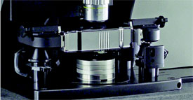
Figure 1 - Crystal Scanner (center) shown mounted directly onto the Nano-R AFM system.
The Crystal Scanner incorporates
substantial developments
in nano-Newton force measurements.
The force sensor is a
small crystal oscillator (Figure 2)
that has a sharp probe mounted
at the end of the crystal. When
the probe (Figure 3) approaches
a surface, the oscillations of the probe are dampened. The
amount of dampening is dependent
on the force between the probe and the sample. Advanced
feedback software is applied to
optimize the oscillation frequency
of the probe and the
amount of resultant force
between the probe and the sample
while the surface of the sample
is scanned.
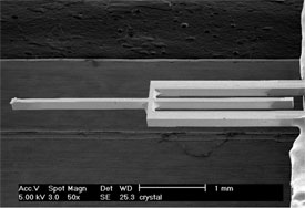
Figure 2 - SEM image of the quartz crystal oscillator used in
the Crystal Scanner.
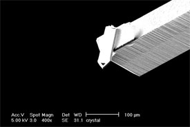
Figure 3 - SEM image of cantilever assembly glued to the
quartz crystal oscillator.
A key benefit to this approach is
that there are no mechanical
adjustments needed for the crystal
sensor’s operation. This is in
contrast to a conventional AFM
that uses a laser, which first must
be focused onto a very small area
on the back of the cantilever.
This reflected signal must then
be manually focused onto a photodetector,
in which position is
critical to the clarity and accuracy
of the resulting image. This
not only saves time, but also
requires less training for a new
user, making the system more
routine in operation.
The quality of the images produced
is also improved. The Crystal
Scanner used with the flexure piezo-scanner
design combined with real-time scan linearization produces a system
with minimal cross-talk between
scan axes, with the resultant images
showing little or no background bow.
This is particularly important when
studying large, flat areas such as a silicon
wafer or a glass panel. This was
the most important design goal for the
AFM products—to produce a system
that is more than a basic imaging tool,
while making it as easy to use as a scanning electron microscope.
System technology
In looking at current AFM users, it is
clear that while there are researchers
doing fundamental science with the
microscope, most users just want
rapid results that are quantitative,
repeatable, and precise. For example,
the operation of an analytical services
laboratory where samples may vary
day to day but may be studied using
standard imaging protocols demands
an instrument that is easy to use but
that also delivers repeatability on a
daily basis. This means that the system
must be straightforward to use
without the incumbent artifacts
associated with the skill-intensive
older designs of instrumentation. This
is provided with the Point and
Scan™ technology employed with
the Crystal Scan software. It features
on-board video tutorials that coach
the operator through the setup, image
capture, and analysis procedures.
Again, this meets the ease-of-use
design criteria. With advanced algorithm
libraries built into the software
platform to establish probe quality,
even the scan parameters may be
optimized, removing the uncertainties
of the setpoints associated with
light lever systems. Together, these
benefits provide the reliability of
quality images each time the system is
used. The system even alerts the operator
to change the probe if it is not
suitable or out of specification.
Whether users are in an academic
research environment or in an industrial
analysis laboratory, today’s
demand is for routine nanoscale measurements
with a key driving requirement
for today’s imaging tool being
the ability to provide results faster
with minimal time required to learn
the technique. Analogous to scanning
electron microscopy, Crystal Force
Microscopy (CFM) provides the user
with an instrument for tabletop
metrology and imaging.
A nonscientific issue is also becoming
more relevant when selecting an
instrument: Cost of ownership is an
area that is becoming very important
in deciding which instrument to
choose. It is not merely the price paid
to put the instrument onto the bench,
but also it may be necessary to hire a
highly skilled operator to fully appreciate
the light lever design of an AFM.
However, with the simplicity yet utility
of the Crystal Scanner approach,
new users of AFM have access to a
cost-effective high-resolution metrology
microscope with applications in
many areas.
In metrology, the study of optical
media such as DVDs has required the
ability to measure the physical dimension
of features at the nanometer
level. The study of masters, stampers,
and replicas is now routine using
AFMs. Use of Crystal Scanner technology
makes this a rapid and simple
task with specialized software to calculate
and produce customized reports
from a single keystroke.
The entire field of nanotechnology is
exploding and with it is the need to be
able to characterize the materials
being used at the nanometer scale.
Nanotubes, which are finding use in
sensor applications, may be visualized
using the Crystal Scanner. They may
be quantified in terms of length and
diameter as well. Particle & Grain
Analysis software (Particle Nanotechnology)
may be used to characterize
nanoparticles in which uniform
size distribution may play an important
role in the end user application.
The size of grains at the nanoscale will
often be a critical component in
determining in-use properties. For
example, the electrical and mechanical
properties of many thin films are
directly affected by grain size.
Conclusion
The manufacturer made a conscious
decision in the design of its scanning
technology for AFMs: to produce a
system that makes metrology measurement
at the nanoscale a routine task.
The AFM has been described by many
as one of the “picks and shovels” tools
for the enabling of nanotechnology.
With research in academia and industry
focusing a great deal of development
and investigative resources in
this area, Crystal Scanner technology
is poised to play an important and pioneering
role for many years to come.
Additional background reading
Binnig G, Quate CF, Gerber C. Phys Rev Lett 1986; 56:930.
Meyer G, Amer M. Appl Phys Lett 1988; 53:1045.
Tortonese M, Barrett RC, Quate CF. Appl Phys Lett 1993; 62:834.
Pohl WD. US patent 4851671 (1989).
Günther P, Fischer UC, Dransfeld K. Appl Phys B 1989; 48:89.
Seo Y, Park JH, Moon JB, Jhe W. Appl Phys Lett 2000; 77:4274.
Seo Y, Choe H, Jhe W. Appl Phys Lett 2003; 83:1860.
Karrai K, Grober RD. Appl Phys Lett 1995; 66:1842.
Rensen WHJ, van Hulst NF, Ruiter AGT, West PE. Appl Phys Lett 1999; 75:1640.
Rensen WHJ. PhD thesis, 2002.
Giessibl FJ. Appl Phys Lett 2000; 76:1470.
Weaver Jr W, Timoshenko SP, Young DH. Vibration problems in engineering. New York: Wiley, 1990:366.
Mattila ST, Kiihamäki J, Lamminmäki T, et al. Sensors and Actuators A 2002; 101:1.
Durkan C, Shvets IV. J Appl Phys 1996; 79:1219.
Gregor MJ, Blome PG, Schöfer J, Ulbrich RG. Appl Phys Lett 1996; 68:307.
Albrecht TR, Grütter P, Horne D, Rugar D. J Appl Phys 1991; 69:668.
Edwards H, Taylor L, Duncan W. J Appl Phys 1997; 82:980.
The authors are with Pacific Nanotechnology,
Inc., Technology Center, 17981 Sky Park Circle,
Ste. J, Irvine, CA 92614, U.S.A.; tel.:
949-253-8813; fax: 949-253-8816; e-mail:
[email protected].