Modern scanning electron microscopes (SEMs) offer vast improvements over early models in terms of electron optics, detector design and computing technology. They are easier to maintain and use and in some cases have gotten smaller. Instruments such as the NeoScope (Figure 1, bottom) (JEOL, Peabody, Mass.) can be placed on a laboratory bench and offer upper magnification limits at 60,000×, translating to a resolution of better than 20 nm. This evolution in SEMs has led to their use across a variety of disciplines, among them pharmaceutical, food processing, forensics, materials engineering, energy and semiconductors.
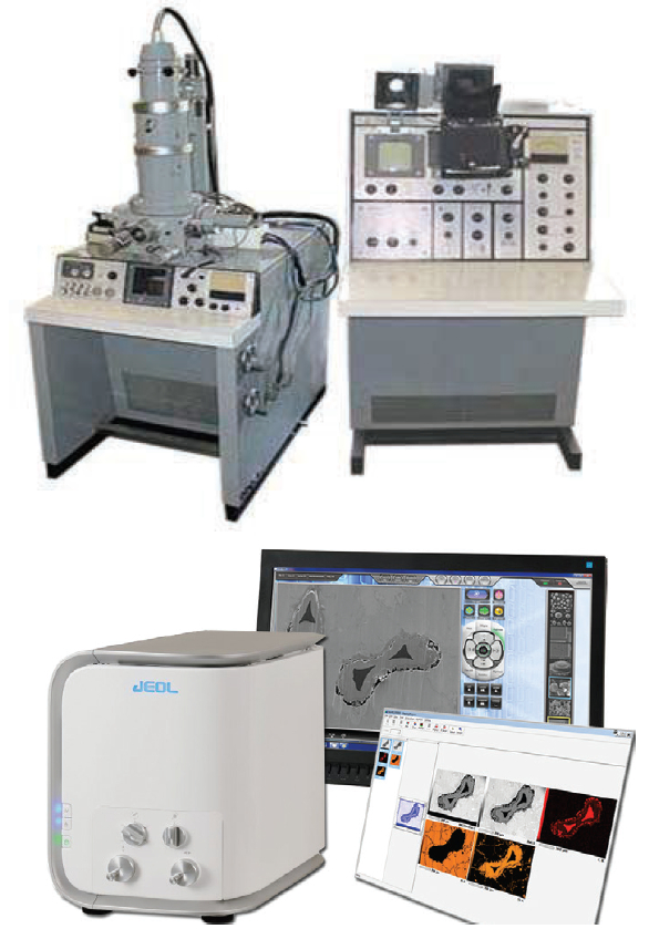 Figure 1 – Top: JSM-1—resolution 25 nm, magnification 30,000×. Bottom: NeoScope—resolution <20 nm, magnification 60,000×.
 Figure 2 – SEM at the user’s fingertips.
It is not unusual for innovations from the scientific community to be adapted and brought to the commercial space. With the InTouchScope series of SEMs, JEOL has reversed the process, adapting commercial multi-touch software control technology and bringing it to scientific instrument operation. Much like operating a tablet or smartphone, the interface of the InTouchScope series breaks down barriers to learning the operation of a complex scientific instrument and increases productivity. Literally all SEM controls are at the user’s fingertips (Figure 2). An embedded color camera further enhances the user experience by allowing the operator to navigate from a color image. ‘Navi’ mode, for less experienced users, provides a step-by-step guide from sample introduction to auto function guided image formation in minutes.
SEMs can be used to examine microstructure at much higher magnifications than are possible with an optical microscope—contemporary SEMs can achieve subnanometer resolution. Even at magnifications that are within the scope of an optical microscope, an SEM has orders of magnitude better depth of field (Figure 3). Whole images can be in focus at high magnification; there is no need to use software to collate a stack of images taken at different focal for fine surface morphology, backscatter electrons for compositional information and X-rays to obtain qualitative, quantitative and spatial distribution of the elements present (Figure 4).
 Figure 3 – Top: light microscope image. Bottom: SEM image.
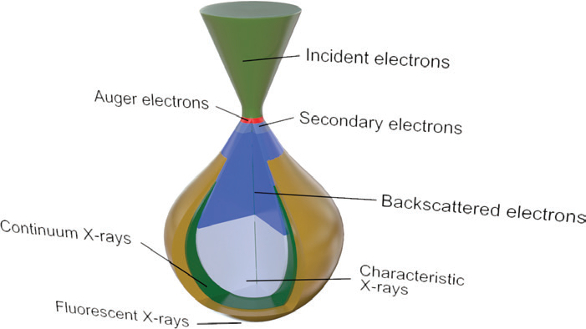 Figure 4 – Signals in SEM.
 Figure 5 – Color navigation image on InTouchScope.
In one example of how common signals can be used, Figure 5 shows a color image of wires from a medical device in cross-section. The user can click on the image to choose the wire for SEM imaging and analysis, and the SEM sample stage will automatically drive to that position. Cross-hairs on the color image will display the location being viewed in the SEM. Next, imaging with two detectors simultaneously will provide information that can be helpful in understanding composition and structure. Figure 6 shows a secondary electron image of the wire and a backscattered image. The surface morphology of the polymer coating on these wires is easily seen, with the secondary electron image (top) and the backscatter electron image (bottom) showing bright particles within the polymer coating that would be indicative of some higher atomic number material that is not seen with the secondary image. Further examination by energy dispersive X-ray (EDS) analysis indicates these small particles are composed of tungsten (Figure 7).
 Figure 6 – Cross-section of wire. Top: secondary electron image. Bottom: backscatter electron image.
 In the pharmaceutical industry, products are required to be free of foreign particles. If visual inspection reveals particles, they must be characterized. Some common foreign particles that might be found in a parenteral drug are glass, rubber, fibers and metal fragments. These can be quite small (<50 μm); SEM coupled with EDS offers a fast, nondestructive method of evaluation. The example in Figure 8 shows a particle fragment typical of what might be found. Morphology and size are easily observed, and X-ray analysis reveals the composition contains Fe, Ni and Cr, which would be indicative of a type of stainless steel.
SEM often provides complementary information to other techniques such as mass spectrometry or NMR (nuclear magnetic resonance) in the characterization of materials. Since it is nondestructive, SEM provides a quick way of surveying a material before undertaking other analyses. In the following example, an unmarked tablet was first analyzed using an open air ionization source (DART) (JEOL) mass spectrometer. From the positive ion mass spectrum of a methanol extract, evidence of picolinic acid was found (Figure 9). However, within this spectrum there was a mass defect at m/z 419.0211 that was not readily identified. NMR analysis showed mostly aliphatic compounds and negative ion mass spectrum corroborated this evidence with peaks relating to fatty acids, stearate and palmitate (Figure 10). These are common excipients and not unexpected in a tablet formulation. Examination of the tablet was continued with the SEM (Figure 11). The backscatter electron image showed a heterogeneous structure. Further EDS analysis identified the bright regions to be high in Ca and P, which is indicative of calcium phosphate, also a common excipient used as a diluent in pharmaceutical tablets. Spatial distribution of the calcium phosphate and the fatty acid excipients are shown in both the backscatter electron image and in the EDS hyperspectral maps. However, NMR and SEM did not show data that would help elucidate the mass defect at m/z 419.0211. Therefore, paper spray mass spectrometry was used in order to look for trace levels of inorganic compounds, and the result showed evidence of chromium (Figure 12). Searching the NIST database, a match was found with chromium picolinate, a common chromium dietary supplement (Figure 13).
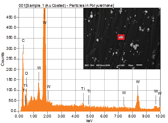 Figure 7 – Backscatter electron image (inset) and EDS spectrum of particles in wire coating.
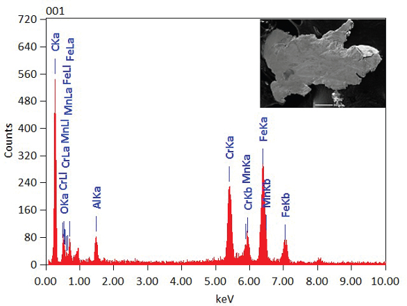 Figure 8 – Secondary electron image (inset) and EDS spectrum of foreign particle from parenteral drug.
 Figure 9 – DART MS of methanol extract of unknown tablet.
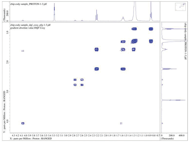 Figure 10 – 2-D NMR of methanol extract of tablet.
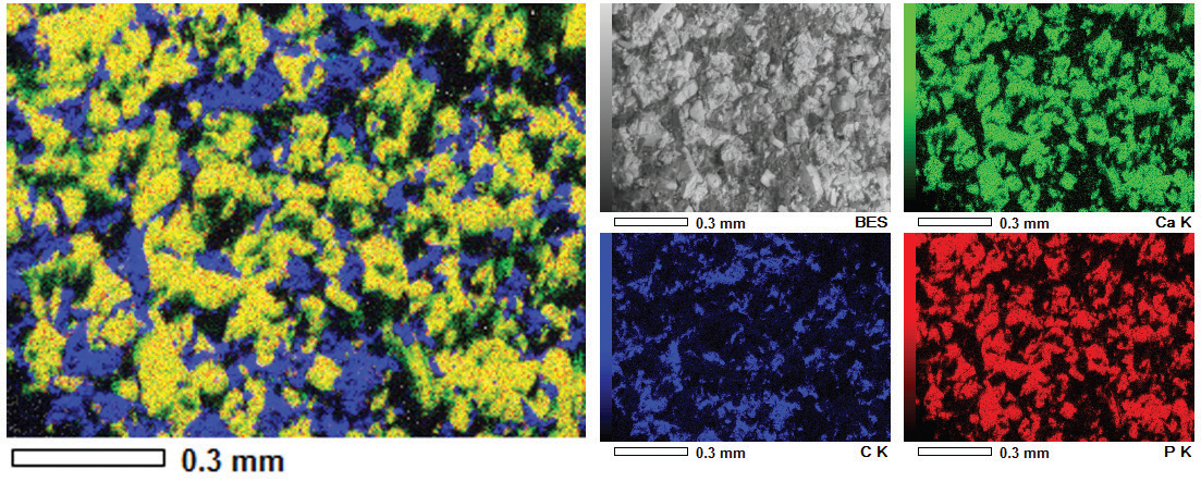 Figure 11 – Backscatter electron image and EDS hyperspectral map data of tablet.
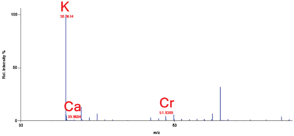 Figure 12 – Paper spray MS of methanol extract.
 Figure 13 – Chromium picolinate
 m/z
: 419.020949.While no single technique could fully characterize this tablet, SEM, MS and NMR together gave insight into the tablet’s formulation.
Donna Guarrera is assistant director, SM Division, JEOL USA, Inc., 11 Dearborn Rd., Peabody, Mass. 01960, U.S.A.; tel.: 978-535-5900; e-mail: [email protected]; www.jeol.com