Thin-film solar cells (TFSCs) have developed into a highly efficient source of energy in solar cell technology, due to the reduction in semiconductor material required compared to traditional solar cells. Efficiencies of thin-film solar cells are now approaching 20%, and optimizing the performance and manufacturing process of TFSCs has become vital.1 Assessing the uniformity of each thin film within the solar cell is an important part of optimizing that efficiency. Since defects or nonuniform thin films can lower the efficiency, it is important to be able to quantify the thickness and composition of the layers over a given area. Micro X-ray fluorescence (micro-XRF) spectroscopy is one technique that can be used for this application.
Properties of thin-film solar cells and current measuring techniques
TFSCs are categorized based on the photovoltaic (PV) material used, such as copper, indium, gallium, selenium (CIGS), or cadmium-telluride (CdTe), and are typically 1.5–2 μm. These PV materials are commonly sputtered onto a metal contact layer underneath, typically no more than 0.5 μm, which is supported on a glass or metal substrate.2 The uniformity of the composition and thickness of these layers are crucial factors, since performance is known to degrade with variation. Thus, knowing how the thickness and composition of each layer behaves can allow manufacturers to determine where the process may require improvement. Figure 1 shows a typical arrangement of thin films for a CIGS thin-film solar cell.
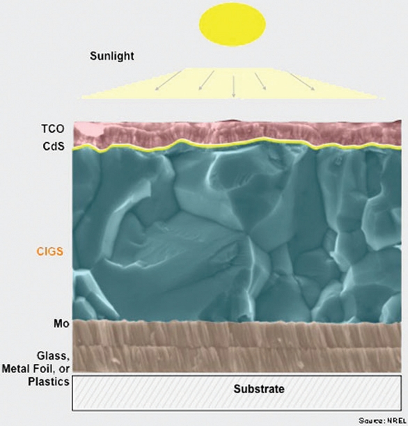 Figure 1 – Typical arrangement of thin films for a CIGS thin-film solar cell. (Courtesy of National Renewable Energy Laboratory [NREL], Golden, CO.)
Measurements to assess the PV material (i.e., CIGS) will be done before the upper layers (transparent conducting films [TCO] and CdS) are deposited. Examples of common techniques used to attain this information include reflectance spectrometry, which measures light absorption over a range of wavelengths to measure the layer thickness, and can also assess the surface roughness properties.3 Inductively coupled plasma (ICP) spectrometry requires digestion of the material to assess the composition of each layer individually.4 Bulk XRF (large spot technique) and handheld XRF units can be used to quantify the composition and thickness of the layers, but the large spot size prevents any distributional information (uniformity) from being provided. However, micro-XRF is unique in that it is capable of nondestructively measuring both the thickness and composition simultaneously, while still observing the uniformity of each.
What makes micro-XRF useful?
Micro-XRF is an elemental technique that uses X-ray tube emissions to generate characteristic X-ray fluorescence from the sample, providing detection for sodium (Na) and heavier elements. Unlike bulk XRF, which offers a relatively larger spot size oriented upwards, micro-XRF focuses or collimates the X-ray beam to significantly smaller spot sizes, ranging from ~30 μm to 2 mm, and typically orients the beam down on the sample.
One advantage to micro-XRF is the nondestructive X-ray beam, which means that the sample does not need to be digested (such as ICP) and will not be damaged by the excitation source. In addition, using an X-ray beam provides sufficient power to penetrate far enough into the sample and excite all of the layers, including the substrate. This is not possible with weaker excitation sources, such as an electron beam. Also, the X-ray beam is focused down to small spot sizes with either a glass capillary or a collimator, enabling measurements to be taken from much more localized areas. Coupling this with a navigable XYZ stage allows for distributional measurements by rastering over a two-dimensional area, as opposed to having one large spot average out that same area, as with bulk XRF.
In addition, micro-XRF is particularly advantageous because it can measure both the composition and thickness simultaneously. The main requirement to employ micro-XRF for thin-film measurements is that the user must know what elements are contained in which layer. In the application of TFSCs, the stacking arrangement is almost always known. Since the quantification is based on measured intensities from the fluoresced elemental lines, internal modeling within the software is able to correct for interlayer effects and therefore calculate both thickness and composition at any given sampling point. Additional bulk and thin-film standards can be used to further improve the modeling accuracy. This quantitative capability allows generation of three-dimensional profiles to fully assess the uniformity of the solar cell.
Micro-XRF method of quantifying thin-film thickness and composition
Once the X-ray source (Bremsstrahlung) generates the elemental lines off the TFSC, the spectrum is then run through a thin-film quantitative routine. Typically, these routines can handle up to about five alloy layers, with about 10 elements in each layer. This routine does require knowledge of which element is located in which layer. Once that is determined, the routine will use the measured elemental intensities to quantify the thickness and composition.
Thickness is determined based on the intensity ratio, or the ratio of the measured thin film versus the theoretical bulk intensity for that element. The thicker the layer, the closer the ratio will approach one. Thinner layers will conversely approach zero (see Figure 2). Furthermore, it will model accordingly for interlayer effects, which is when one layer can cause secondary fluorescence in the layer(s) above it. As mentioned, these results can be further calibrated with the use of bulk and/or thin-film standards, which will correlate known values to theoretical intensities to significantly improve the accuracy of the results.
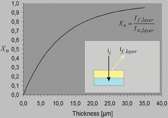 Figure 2 – Graph showing the behavior of intensity ratio vs thickness. If an element has an “infinite” thickness, the X-ray beam will not penetrate through the sample. The respective intensity is labeled I∞. If that same element is in thin-film form, the X-ray will penetrate through and generate reduced intensities. This is labeled If. The ratio of these two values as the sample goes from thin to infinite is represented in the graph.
CIGS/Mo/glass example
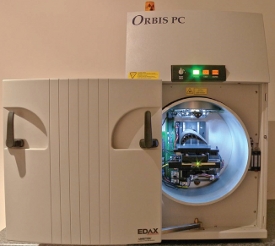 Figure 3 – Orbis PC Micro-XRF spectrometer used for the measurement of the CIGS/Mo/glass sample.
To illustrate the capabilities of micro-XRF for measuring TFSCs, a segment of a real solar cell was used. In this example, the spectrometer used was an Orbis PC (EDAX, Mahwah, NJ).
This micro-XRF unit was equipped with a 50-W, rhodium-anode X-ray tube, and a 30-mm2 silicon drift detector (see Figure 3). The benefit of the Orbis is that it allows selection of up to three different spot sizes, ranging from microns to millimeters. In this case, the 1-mm collimator was used.
Another advantage of this unit is the inclusion of primary beam filters, which are integrated with the software’s quantification routine. A thin aluminum filter was used to eliminate the Rh(L) tube scatter artifact peaks, which would have interfered with sulfur. Additionally, all samples were measured under low vacuum to optimize light element sensitivity.
The sample being measured was a CIGS-type solar cell, which had two thin films on a substrate. The top PV material was CIGS, or copper-indium-gallium-selenium/sulfur. The second metallic layer underneath was pure molybdenum (Mo), and the substrate was a float glass. The goal with this sample was to assess the uniformity of the thickness and composition to observe the quality of the sputter coating process. Therefore, the measurements were more focused on the edges and corners. A 40 × 40 mm portion near the corner of the panel was analyzed by setting up an automated raster of 35 × 35 points, using the 1-mm collimator for collection. Each point was collected for 30 sec.
As mentioned previously, these layers typically have an expected thickness range of <0.5 µm for the Mo layer, and typically 1.5–2 µm for the CIGS layer. Given these ranges, it is now possible to choose an appropriate standard. While both bulk and/or thin-film standards can be used, this example employed only one thin-film standard. The standard was stacked exactly like the unknown samples, and also had certified thickness and composition values, which were in the approximate range of our unknowns. The standard had 18.9 atomic percent (at%) Cu, 15.9 at% In, 4.9 at% Ga, and 60.3 at% Se. The CIGS layer was 2.15 µm, and the pure Mo layer was 0.28 µm, on a float glass substrate. Correlating these known values with the calculated intensities significantly optimizes the accuracy.
After collecting the 35 × 35 raster of points and running them through the thin-film quantification routine, the values for each layer were then plotted out to observe the uniformity. Figures 4 and 5 show some select results.
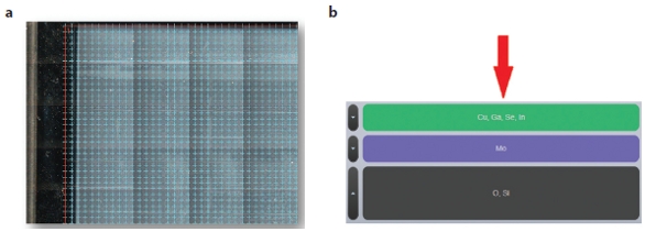 Figure 4 – a) Measurement area on the CIGS sample. The 35 × 35 matrix is represented with the red and blue markers. After that is collected, the software defines each layer (b), where the elements’ location must be known. The incoming X-ray will measure the whole sample at once, and will use the characteristic lines to calculate thickness and composition.
 Figure 5 – a) Thickness plot of the entire top CIGS layer. b) Atomic percent of just the Se content in the CIGS layer. c) Thickness plot of the lower Mo layer.
CIGS/Mo/glass discussion and conclusions
One of the interesting observations from Figures 4 and 5 is the comparison of the CIGS thickness versus the selenium composition. The CIGS thickness shows significant tapering near the edges and especially the corner, where the thickness drops away from the 1.3–1.4 μm range closer to the center. However, the Se composition is relatively uniform, and does not vary much beyond the 52–26 at% range. This would suggest that while the CIGS material is relatively homogeneous in composition, the sputtering process itself did not deposit a very uniformly thick CIGS layer. Likewise, the Mo layer underneath also shows the same tapering effect near the edges, but also shows a lateral “striped” pattern of varying thickness, between approximately 0.24–0.28 μm.
This type of information is highly valuable to refining the manufacturing process. Currently techniques do exist that can measure thickness or composition of TFSCs, some of which require sample destruction (digestion), or large sampling areas. The benefit of micro-XRF is that it can successfully quantify both of these values independently based off a single spectrum. In addition, the small spot allows more localized areas to be analyzed, as opposed to averaging a larger area. Coupling the small spot size with an XYZ navigable stage allows two-dimensional rastering and scanning, which facilitates assessment of the thickness and composition uniformity.
References
- www.nrel.gov/docs/fy08osti/42539.pdf.
- www.nrel.gov/pv/thinfilm.html.
- www.nrel.gov/docs/fy05osti/37061.pdf.
- www.nrel.gov/docs/fy02osti/31739.pdf.
Andrew Lee is an Applications Engineer for micro-XRF, EDAX Inc., 91 McKee Dr., Mahwah, NJ 07430, U.S.A.; tel.: 201-529-6117; e-mail: [email protected].