Tip-enhanced Raman spectroscopy, or TERS, integrates scanning probe microscopy (SPM) for nano-scale imaging with confocal Raman spectroscopy for chemical characterization. Challenges with tip quality, optical alignment, consistency and speed, however, have made the technique difficult and complex. New instrumentation is addressing these challenges, allowing TERS to migrate from pure research to routine laboratory analysis. These systems provide correlated nano-scale Raman imaging, enabling scientists to visualize, chemically characterize and implement change, even at the single-molecule level. As a result, TERS is extending nano-Raman imaging applications from conventional polymers and industrial constituents to a wide array of organic molecules,1 as well as to the more unusual carbon-based,2 two-dimensional3 and semiconducting nanomaterials.4 In the life sciences, TERS is expanding into the investigation of nucleic5 and amino acids.6
TERS bridges the gap to nano-Raman
Raman spectra are generated by inelastic scattering resulting from the interaction between the excitation beam and the chemical bonds in the sample.7 Since Raman is a far-field optical technique, its spot size is diffraction-limited, typically on the order of a few hundred nanometers to 1 micrometer. As a result, it is restricted to micro and macro applications.
SPM, on the other hand, is the tool of choice for examining the nanoworld. Providing over 40 different measuring modes, it not only images topography, magnetic domains or local electrical fields (e.g., voltage, resistance, capacitance, surface potential), but can image and quantify a variety of force interactions, including friction and the difference in hardness or tacticity between phases. If the probe tip is functionalized, it can also visualize antigen/antibody or drug/target interactions. However, it cannot provide a chemical spectrum and, until recently, was limited by slow scan speeds.
TERS combines Raman with SPM, coupling nano-scale chemical characterization to SPM imaging (see sidebar). The concept of combining imaging with chemical analysis is familiar to electron microscopists, who routinely overlay elemental analysis maps onto a scanning electron microscope (SEM) image. For spectroscopists, the additional imaging offers a new dimension to chemistry.8
New generation TERS instruments
Two of the most common approaches to TERS are confocal Raman systems with single atomic force microscope (AFM) objectives and “TERS ready” systems in which a Raman manufacturer provides a port for an SPM interface. In contrast, the instruments described in this article are designed specifically for TERS, integrating both the software and hardware from the SPM and the spectrometer.

For routine studies of materials and nanomaterials, the SmartSPM and OmegaScope coupler (AIST-NT, Novato, Calif.) are combined with the compact XploRA spectrometer (HORIBA Scientific, Edison, N.J.). For the life sciences, there is an inverted microscope version of the XploRA, and, for more demanding applications, a fully automated system built on the HORIBA LabRAM HR Evolution that includes four detectors and high-spectral resolution. Each spectrometer can be integrated with the AIST-NT TRIOS platform, which allows complete optical customization.
According to Dr. Marc Chaigneau, AFM/Raman product manager at HORIBA Scientific, “For the first time [these new hybrids] offer reliable Raman enhancement and stable alignment with very short acquisition times, freeing the technique from the need to subtract far-field from near-field and from the potential drift issues inherent in SPM technology.”
True TERS imaging
 Figure 1 – True hyperspectral nano-scale Raman imaging of an isolated carbon nanotube (CNT). Raman resolution: 8 nm; scan area: 100 nm × 100 nm; scanned in 1.3-nm steps at 100 msec/pixel; scan time: <9 min.
Simply overlaying an SPM image with a Raman map is not true nano-Raman imaging. A typical test to prove that TERS is working compares Raman intensities with the TERS tip up versus the tip down. The increased signal from this approach can be misleading. Reflections from the bottom of the tip can cause moderate increases in the Raman signal that are not true TERS.
The nano-Raman image is a better test. Figure 1 was collected from simultaneous, co-localized SPM and Raman scans, built line by line, rather than overlaid. The result is a true TERS hyperspectral image, with optical resolution below 10 nm and full-range Raman spectra in each SPM pixel.
In this figure, red corresponds to the pure graphite component of the CNT (2D band), while the white shows the imperfection in a defect-related area. The green circle highlights a local lattice defect. The jump in intensity over a single step illustrates the ability to resolve the chemical shift down to 1.3 nm.
Speed, stability and ease-of-use
 Figure 2 – Bolting the SPM and the spectrometer to an optical table forms a stable foundation. (1) SmartSPM with probe holder and sample stage; (2) OmegaScope with (3) two objective scanners; (4) video microscope for SPM navigation; (5) XploRA: full research confocal microscope; and (6) compact, powerful microspectrophotometer for conventional Raman and nano-Raman (TERS).
The image in Figure 1 was taken on a tradeshow floor, under conditions that were far from ideal, without an active isolation table or enclosure. The high resonant frequency of this SPM makes it insensitive to vibration, eliminating the need for cumbersome and expensive anti-vibration equipment. It can be bolted to the same optical table as the spectrometer (Figure 2), enabling unwavering, fixed optical alignment.
SmartSPM
The SmartSPM combines proprietary electronics with stiff XYZ flexure-guided scanners instead of more conventional PZT tube scanners. The results are high resonance frequencies (7 kHz in XY, 15 kHz in Z), elevated stability and precise control.
Integration of the SPM-spectrometer software and synchronized triggering of the electron multiplying charge-coupled device (EMCCD) allows fast acquisition of calibrated Raman spectra at each pixel, critical for real-time assessment of the surface chemistry at the nanoscale. On average, scan speeds are 10 times faster than other systems, even for scans as large as 100 μm × 100 μm x 15 μm.
Another advantage of faster scanning is a significant drop in drift, a problem with slower tube scanners. Improved feedback controls dampen the ringing that occurs at the bottom of each step. The quicker the ringing is stopped, the sooner the Raman signal can be acquired. Advanced scanning motion control in XY reduces phase lag errors by 10- to 100-fold. This ability to stop and start precisely enables more complex acquisition protocols.
To avoid interference with the Raman laser, SmartSPM uses a 1300-nm laser to track probe motion. Invisible to the human eye, it emits far beyond the typical visible and near-IR wavelengths used for the TERS experiment.
The performance of an SPM depends on the health of the last few nanometers at the end of the tip, and tip health relies on the quality of the probe and proper technique. Approaching a surface too quickly or without the necessary control causes the tip to crash into the surface and break. Also, the tip can become blunt with wear, pick up debris or become contaminated. As described above, the use of stiff XYZ flexure-guided scanners ensures precise control. Open architecture allows quick probe exchange without removing the head or disturbing the sample. Automated tip alignment returns the new tip to the original location, within a micrometer. Similarly, the sample can be exchanged without removing the head or disturbing a well-performing tip.
After tip or sample exchange, the SmartSPM automatically realigns the probe to the detector, expediting the experimental process, ensuring reliability for the next scan, and avoiding cumbersome manual adjustment. Both HORIBA and AIST-NT offer nanogold-tipped probes for AFM-TERS, Omni TERS probes, which are protected silver probes for AFM-TERS, and etched gold wire for STM and tuning fork feedbacks.
XploRA spectrometer
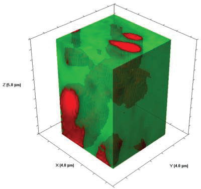 Figure 3 – SWIFT 3D Raman hyperspectral volume display of barium sulfate particles in a polymer matrix. Volume = 92 μm3 . Image acquired with 200-nm steps and 50-msec integration time
.
The XploRA’s robust research-grade confocal microscope (Figure 2, #5) provides the spatial resolution and fluorescence rejection needed for the analysis of even small particles and thin layers. Proprietary gratings, coupling optics and microscope objectives optimize throughput and collection for the selected laser wavelength. For maximum flexibility, the integrated spectrometer has a fully automated four-grating turret (2400 gr/mm, 1800 gr/mm, 1200 gr/mm and 600 gr/mm) and can be equipped with up to three internal lasers (532, 638 and 785 nm). Laser selection is fully automated and requires no moving optics.
Acquisition times of <1 msec/point are possible with the spectrometer’s SWIFT ultra-fast Raman imaging (HORIBA) (Figure 3). SWIFT speeds scan time by minimizing integration time for both far-field scans from XploRA’s confocal Raman microscope and TERS scans from the SmartSPM. Once a scan is complete, individual bands can be selected to elicit specific information without rescanning. Because scans can be completed in a few seconds, routine industrial processes such as polymer curing, which occur on time scales of minutes or hours, can be imaged in real time.
OmegaScope
TERS systems often use a fiber optic coupler to connect the SPM to the spectrometer. In contrast, the integrated TERS instruments use free-space coupling through the OmegaScope (Figure 2, #2), maintaining confocality and maximizing Raman photon collection.
This rigid building block houses the SPM (Figure 2, #1) and the objective scanner (#3) to align the Raman laser to the TERS probe. Its open optical design provides single or simultaneous Raman access through top, side and, optionally, bottom ports; integrates a video microscope (#4) for viewing the sample beneath the tip for optimal navigation to sites of interest; and delivers a solid foundation and positioning stage for the SmartSPM.
OmegaScope uses high-numerical-aperture optics (up to 0.7 NA in top and side channel; up to 1.4 NA in bottom). These high NAs not only maximize XY resolution and optimize confocality to enhance contrast by rejecting out-of-focus light, but collect Raman or TERS signals efficiently. Coupled with fast detection hardware, their improved signal output contributes to faster scan speeds and permits simultaneous acquisition of Raman spectra with SPM images.
Because the excitation laser is built-in, the Raman excitation path is short and simple, eliminating the need for a fiber optic coupler. Routine optical alignment is achieved under computer control using the objective scanner, precisely registering the Raman excitation laser to the TERS tip. The tip acts like an antenna, re-radiating the laser’s energy to form an evanescent field (the hot spot), which interacts with the specimen.
Software and support
While the SPM and spectrometer can operate independently, they are fully integrated using AIST-NT software, which interfaces with the HORIBA LabSpec 6 Spectroscopy Suite to record simultaneous, calibrated TERS spectra at each SPM pixel. The easy-to-use graphical user interface guides the user from experimental setup through acquisition to complete analysis. LabSpec 6’s data processing software includes ParticleFinder, multivariate analysis, 3-D volume and surface rendering, and database searching using the HORIBA edition of KnowItAll (Bio-Rad, Hercules, Calif.). Despite the complexity of the system, field experience demonstrates that most new users are up and running within a day of completing installation training.
Characterizing complex carbon nanostructures
Carbon nanomaterials exhibit exceptional strength, electrical conductivity and heat resistance that make them industrially interesting, and they are getting easier to produce. These materials are allotropes. While each is made of carbon, they have different internal structures that result in properties as different as those of pencil lead and diamonds. The ability to characterize and manipulate carbon nanomaterials has led to their growth, and they now include conventional diamond, nano-crystalline diamond and graphite as well as graphene—single sheets of hexagonally bonded carbon that form the building blocks for a number of other structures. When graphene is formed into a ball it becomes a fullerene (buckyball, C60); when rolled into a tube it produces a single-walled carbon nanotube (SWCNT), with wall dimensions on the order of 1–2 nm thick. Covering a CNT with one or more additional sheets of graphene produces double- or multi-walled CNTs (DWCNT or MWCNT, respectively).
In conventional Raman and TERS, each molecular bond responds to its own vibration, depending on the orientation of that bond within the molecule and the weight of the atoms on either side of the bond. As illustrated in Table 1, carbon bonds are very sensitive to Raman analysis. Less restriction on bonds generates a higher-frequency vibration, while greater restriction results in lower vibration and a downfield shift of the Raman peak.
Table 1 – Carbon nanomaterials and key related Raman signals (Images courtesy of Wikipedia)
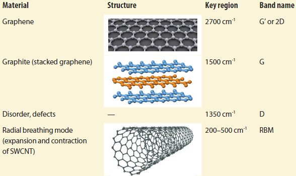
Since the additional graphene sheets in MWCNTs restrict movement, they do not exhibit lateral expansion/compression or radial breathing mode (RBM). Also, the higher number of graphene layers, the greater the potential of disorder or potential defects, resulting in a stronger D band.
Figure 4 illustrates these concepts with the use of true TERS imaging for the nano-scale analysis of a non-ideal multi-component carbon system such as might be found in complex nanomaterials or the life sciences.10,11 The sample is a mixture of GO, SWCNTs and C60 collected under ambient conditions.
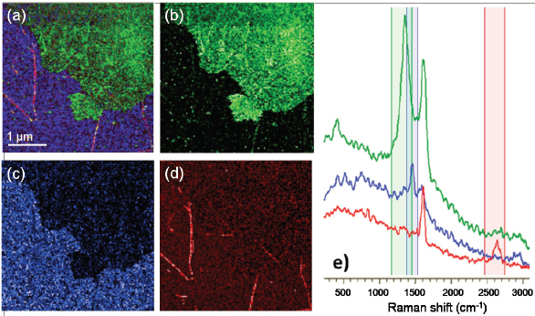 Figure 4 – a) TERS composite image of a complex mix of carbon nanostructures. b–d) Spectra selected for graphene oxide (GO, green), fullerenes (C60, blue) and SWCNTs (red) co-deposited on gold. e) Corresponding spectra. Scan area: 4 × 4 μm, 128 pixels/line; integration time: 100 msec/pixel; lateral resolution: <15 nm. (Image reproduced with permission from Ref. 9.)
Once the full hyperspectral image is recorded (Figure 4a), specific spectral regions can be selected to isolate individual components. GO (Figure 4b) shows a high D band (green, ~1350 cm-1) without a detectable 2D band (2700 cm-1), while SWCNTs (Figure 4d) can be identified by the presence of a 2D band (red). The fullerenes (Figure 4c) were identified by the five-member carbon ring band at 1470 cm-1 (blue) and an organic residue, seen as background, by a C–H band between 2800 and 3000 cm-1.
Conclusion
With the advent of the new integrated systems, TERS is indeed ready, in robust, easily run instruments that are transitioning from the research lab to more routine analyses. On the horizon: new systems to enable imaging in liquids and measuring under high vacuum (<10-8 torr).
References
- Wickramasinghe, H.K.; Chaigneau, M. et al. Billion-fold increase in tip-enhanced Raman signal. ACS Nano 2014, 8(4), 3421–6.
- Mignuzzi, S.; Kumar, N. et al. Probing individual point defects in graphene via near-field Raman scattering. Nanoscale 2015, 7, 19,413–18.
- Voronine, D.V.; Lu, G. et al. Tip-enhanced Raman scattering of MoS2. IEEE J. Sel. Topics Quantum Electron. 2016; doi: 10.1109/JSTQE.2016.2584784.
- Zhang, Z.; Dillen, D.C. Strain and hole gas induced Raman shifts in Ge–SixGe1–x core–shell nanowires using tip-tip-enhanced Raman spectroscopy. Nano Lett. 2015, 15(7), 4303–10.
- Najjar, S.; Talaga, D. et al. Tip-enhanced Raman spectroscopy of combed double-stranded DNA bundles. J. Phys. Chem. C 2014, 118, 1174–81.
- Kurouski, D.; Deckert-Gaudig, T. Surface characterization of insulin protofilaments and fibril polymorphs using tip-enhanced Raman spectroscopy (TERS). Biophys. J. 2014, 106, 263–71.
- Foster, B. Raman microscopy: Taking chemical microscopy to the next level. Am Lab. Apr 2003; http://microscopyeducation.com/raman-microscopy-taking-chemical-microscopy-to-the-next-level_al_apr2003/
- Krayev, A.; Lancry, O. et al. www.spectroscopyonline.com/high-speed-ters-imaging-latest-achievements-nano-raman-spectroscopy
- Krayev, A.; Saunin, S. et al. Fast nanoscale Raman imaging of complex multicomponent samples. Presented at Materials Research Society, Boston, Mass., Nov 2014.
- Sheremet, E.; Rodriguez, R.D. et al. Nanoscale imaging and identification of a four-component carbon sample. Carbon 2016, 96, 588–93.
- Olschewski, K.; Kämmer, E. et al. A manual and an automatic TERS based virus discrimination. Nanoscale 2015, 7, 4545–52.
Barbara Foster is president and chief strategic consultant, The Microscopy & Imaging Place, Inc., 7101 Royal Glen Trail, The “C” Suite, McKinney, Texas 75070, U.S.A.; tel.: 972-924-5310; e-mail: [email protected]. Ms. Foster welcomes comments and questions on her articles. For more detailed technical information on this article, contact Dr. Marc Chaigneau, [email protected].