Recent developments in spectrometer design have made the unique capabilities of X-ray photoelectron spectroscopy (XPS) accessible to scientists and engineers working on the latest devices for energy generation and storage in the renewable sector. Because device design and fabrication are reliant on materials engineering on the nanometer scale, it is important that techniques that are able to achieve chemical characterization on this scale are available. The characterization of two such devices will be discussed here: a copper indium gallium (di)selenide (Cu[In,Ga]Se2, CIGS) solar cell and proton-exchange membrane fuel cells, also known as polymer electrolyte membrane fuel cells (PEMFC).
Precise control of surface, thin-film, and interface composition in these devices is key to device viability and efficiency. XPS delivers crucial insight by providing characterization on the nanometer scale. Accurate characterization of this type is not without its challenges. However, improvements in instrumentation and analytical capabilities have allowed XPS to become a suitable R&D tool. The combination of surface and interface specificity with the ability to analyze a wide range of materials makes the technique well suited to devices that often contain multiple layers of varying chemical composition. Most modern devices such as solar cells rely on the use of a combination of conductive, semiconductive, and insulating layers. Few analytical techniques have the ability to analyze all of these material types in a single analysis session.
What is XPS?
It is useful first to review some of the basic principles of this powerful technique. As the name implies, XPS relies on the photoelectric effect, in which an X-ray photon removes an electron from an atom or molecule provided that photon has sufficient energy. The kinetic energy of that electron depends on the photon energy and the energy required to remove the electron (the binding energy) according to the following equation:
Binding energy (BE) = photon energy
(hυ) – kinetic energy (KE)
In an XPS spectrometer, it is KE that is measured. Typically, a monochromatic X-ray source of a known energy (e.g., AlKα radiation hυ = 1486.6 eV) is used in the excitation. This allows BE of the emergent electron to be easily calculated from the above equation. From BE, it is possible to determine not only the elemental composition of the surface, but also the chemical state of the elements in the material.
The emitted electrons travel a considerable distance in the spectrometer before they reach the detector; thus, to ensure that losses due to collisions with gas molecules are kept to a minimum, XPS spectrometers are operated under ultrahighvacuum conditions. Any solid sample that is compatible with these conditions can be analyzed. All elements except for hydrogen and helium can be detected. Typically, the detection limit of the technique is approx. 0.1 atomic percent.
Figure 1 - K-Alpha XPS spectrometer.
XPS spectrometers are available in a number of forms. Figure 1 shows the K-Alpha system (Thermo Fisher Scientific, Waltham, MA), an example of a modern, highly automated spectrometer. This is the type of instrument used for the analyses described here.
Why is XPS surface specific?
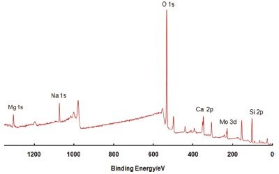
Figure 2 - An example of a survey spectrum. This spectrum is from a CIGS device following a sputter-depth profile (described later).
When X-rays strike a solid, they penetrate the material to a great depth, causing photoemission along their entire path of travel. However, as the photoelectrons travel through the material, they undergo inelastic collisions. Only photoelectrons originating close to the surface (within the top 5−10 nm, depending on the material) stand a chance of escaping without energy loss. The XPS spectrum consists of sharp peaks on a broad background (Figure 2). Electrons generated close enough to the surface that can escape without energy loss contribute to the peaks, while those that escape, having lost some energy, contribute to the spectrum background. XPS is considered to be a standardless technique, providing quantitative results rapidly with little or no sample preparation.
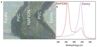
Figure 3 - a) Optical image of the prepared MEA sample. b) C 1s spectrum from the Nafion® (E.I. du Pont de Nemours Co., Wilmington, DE) and epoxy regions of the sample.
Various types of measurements can be made, the simplest being spectroscopic analysis (Figure 3); such measurements can be made from areas down to approx. 15 µm in diam. Imaging XPS is possible using a number of techniques; here it is possible to obtain elemental or chemical state images with a resolution of <3 µm. If XPS measurements are interleaved with etching using a beam of ions, then it is possible to produce a concentration depth profile. This makes it feasible to determine the composition of films that are much thicker than the escape depth of the electrons.
Characterization of fuel cell components using XPS
The first example of how this powerful technique is utilized concerns the analysis of a PEMFC.These devices are currently being developed for both stationary fuel cells and for transport applications.They operate with high conversion efficiency at much lower temperatures than the solid oxide type of cell (typically <100 °C),which makes them capable of rapid startup.
At the heart of these devices is a membrane electrode assembly (MEA). The MEA has layers of platinum in carbon black, which catalyze the reaction of hydrogen and oxygen. A polymer electrolyte (which is typically Nafion) separates the anode and cathode. In MEA manufacture or development, the aim is to maximize the surface area of platinum that is electrically connected to the conducting support; loss of surface area decreases the efficiency of the device. Platinum loss can occur when high currents effectively corrode the carbon-black support, liberating the active metal and allowing it to migrate to the adjacent polymer electrolyte. Additionally, the presence of platinum in the Nafion hinders hydrogen ion mobility in the electrolyte. This article describes how an XPS analysis of an MEA can determine whether platinum has migrated from the catalytically active layers into the adjacent Nafion electrolyte.
Results
Because MEA layers are too thick for conventional XPS depth profiling, sectioning is required for XPS analysis. A 90° cross-section would reveal layers that are too small, and it would not be possible to detect subtle diffusion of the platinum from one layer to another. A solution to this problem is to mount the sample in epoxy and use ultralow-angle microtomy (ULAM). The MEA is then cross-sectioned at an angle of 1 or 2°, allowing the analyst to obtain effective depth information by imaging the cross-section. The dimensions of the ULAM-sectioned layers are now large enough compared to the X-ray probe area that it is possible to have many data points per layer. Figure 3 shows an optical image of the prepared sample in the analysis position of a K-Alpha instrument.
Figure 3b shows the C 1s region of the XPS spectrum from the Nafion and epoxy areas of the sample. The Nafion spectrum has a strong peak associated with CF2 groups in the polymer. It also has a peak at lower binding energy associated with adventitious carbon contamination. The epoxy spectrum has components associated with aromatic and aliphatic carbon and also due to ether and carboxyl type bonding.
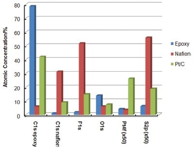
Figure 4 - Quantitative analysis results from the three regions of the sample.
XPS was used to quantify the elemental composition of the MEA-ULAM sample at different areas on the surface. Figure 4 shows the results of the quantification. Fluorine and sulfur were observed in the catalyst layer. This is expected since a small amount of Nafion was mixed into the platinum–carbon layer during manufacture, and Nafion itself contains a small amount of sulfur. Although sulfur is not a contaminant in the platinum layer, these results demonstrate the capability of the XPS tool to detect potential contaminants at low concentration.
The concentration of platinum in the catalytically active layer is less than 0.5 atomic percent, and thus it is necessary to use a high-performance XPS tool to detect it. Even at low concentration, a high-quality signal-to-noise spectrum was acquired from the catalyst layer. In the middle of the Nafion layer, there was no detectable platinum.
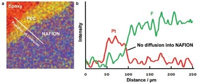
Figure 5 - a) Overlay of two high-resolution XPS images from Pt and F. The white line indicates the position of the linescan shown in (b).
High-resolution XPS imaging was then used to check for diffusion on a much smaller scale. Figure 5 shows an overlay of XPS images from fluorine and platinum from the epoxy, platinum, and Nafion layers. A linescan across the imaging data in the figure shows the profile of platinum and the fluorine from the Nafion. There is no evidence of diffusion of the platinum into the Nafion. It can therefore be concluded that the catalytic effect at the anode and cathode on this sample is not detrimentally affected by loss of platinum into the Nafion.
Compositional analysis of advanced solar cells using XPS
Solar cells based on CIGS thin films have demonstrated very high efficiencies and offer the potential of an economical alternative to bulk, silicon-based solar cells.
 Figure 6 - Depth profile of a CIGS solar cell.
CIGS solar cells consist of a thin-film stack on a substrate, typically glass (Figure 6, inset). The molybdenum and the zinc oxide layers form the electrical contacts. The p-type CIGS film acts as the sunlight absorber layer, with a thin n-type CdS layer forming a p–n junction. The most common manufacturing methods involve evaporation or sputtering of the components. Vaporized selenium reacts with the metals in order to establish the final film composition.
One of the major challenges in producing these devices is to control the film composition. Reproducibility of layers in commercial volumes has been problematic. This is critical because the electrical properties of the cell depend on the exact composition of the layers. Depth profiling with XPS can determine both the composition through the device and the interfacial chemistry. This is essential for understanding how to control the band gap to provide efficient operation. The K-Alpha XPS was used to obtain a composition depth profile from a CIGS sample. Argon ions were used to sputter profile the sample. The depth calibration was checked using the scanning electron microscopy (SEM) image of a cross-section of the sample.
Results
The results of the depth profile of a thin-film CIGS solar cell can be seen in Figure 6. The profile clearly shows the structure of the solar cell: the upper ZnO layer, the thin CdS layer, the CIGS layer, and the Mo substrate. The profile also shows that there are composition gradients of gallium and indium in the CIGS layer, which may influence the band gap of the material. The results prove K-Alpha’s ability to sputter complex multicomponent films while maintaining very good depth resolution throughout the profile.
A change in stoichiometry of the layer near the interface can also be seen. This is probably caused by interaction with the lower layers and could be important to device performance.
Summary
A CIGS solar cell was depth profiled using the K-Alpha XPS instrument. The multilayer structure of the solar cell can be easily determined using this technique, identifying and quantifying elemental components as a function of depth. This type of information is applicable for all thin-film photovoltaic devices. The excellent depth resolution of the acquired data enables accurate characterization of the interfacial chemistry.
Dr. White is Sales and Marketing Manager for Surface Analysis Products, and Dr. Wolstenholme is Regional Sales and Marketing Manager for Surface Analysis Products at Thermo Fisher Scientific, 81 Wyman St., Waltham, MA 02454, U.S.A.; tel.: 781-622-1000; fax: 781-622- 1207; e-mail: [email protected]. The authors would like to acknowledge Dr. Daniel Abou-Ras, Helmholtz-Zentrum Berlin für Materialienund Energie (formerly Hahn-Meitner-Institut Berlin), Berlin, Germany, for supplying the solar cell sample and for helpful discussions, and Dr. Harry Meyer III, Oak Ridge National Laboratory, Oak Ridge, TN, U.S.A., for supplying the ultralow-angle microtomy (ULAM) prepared membrane electrode assembly (MEA) samples and for helpful discussions.