Used in a wide range of products and devices, complex, multi-layered materials have traditionally been based around metallic or oxide layers. Now, with the drive toward lightweight and less expensive components, polymer-based materials are being used more frequently, particularly in areas like display technologies, biomedical devices and energy generation. Understanding how these layers interact with each other and the environment is a critical part of the development cycle. Because these interaction zones are typically just a few nanometers thick, surface-sensitive techniques are required that can profile through the material to access subsurface interfaces.
X-ray photoelectron spectroscopy (XPS) is widely used to study the surface and layer chemistry of materials. The surface sensitivity of XPS provides a powerful analytical platform to probe ultrathin layers. The information obtained in a standard XPS experiment comes from within the top 10 nanometers of a material, roughly 20–30 atomic layers, the region that can impact such properties as electrical performance or adhesion. It also gives direct access to quantitative, chemical state characterization, as opposed to purely elemental information.
Beyond the surface, the interaction of individual layers can have a profound effect on a device’s performance. As an example, reflection of the infrared component of sunlight by architectural glass is controlled by several layers of metals and oxides applied to the outer layer of the glass sheet. This stack is usually around 100–200 nm thick. A process known as depth profiling is used to analyze these types of materials, and involves interleaving cycles of ion beam etching with spectroscopy to build up a layer-by-layer picture of the sample structure. Most XPS instruments include an ion gun that produces monatomic argon ions (Ar+) for this purpose. A range of beam energies are usually available, typically from a few hundred eV up to a few keV, allowing operators to choose etch rates depending on the thickness of the layers to be analyzed. Spectra are collected after each cycle of material removal by ion milling to generate a depth profile, typically displayed as atomic concentration, which shows the variation in the chemistry with depth into the surface. Depths up to a few microns can be investigated using this approach.
The process works particularly well for most inorganic materials, and keeps the chemical structure intact as layers are removed by ion bombardment. However, the types of layer structures that are now being developed for applications such as biosensors, display screens and energy generation depend on mixtures of polymers, metals and oxides. Polymers and some oxides can be damaged by interaction with a monatomic ion beam, changing the material’s chemistry and distorting test data.
The key to minimizing damage to a polymer system during depth profiling is to reduce the energy going into the surface. With a monatomic beam, any energy not used to eject material from the surface generally penetrates into the surface, breaking bonds and damaging the remaining material. This damage is typically just greater than the XPS information depth, so spectra become representative of the damaged surface rather than the real surface. It is possible to minimize the damage zone by reducing the beam energy, but below a threshold of around 50 eV, it no longer has an effect on the surface.
An ion source that sputters the sample surface using large, singly charged gas clusters was developed to address this. The monatomic and gas cluster ion source (MAGCIS) for Thermo Scientific XPS instruments (Thermo Fisher Scientific, East Grinstead, U.K.) uses both Ar+ and Arn+ (50 ≤ n ≤ 2000) gas cluster sputtering, enabling both surface cleaning and depth profiling of the growing class of advanced materials built from mixtures of organic and inorganic compounds. The technique helps to negate the low-energy sputtering threshold by making the projectile much heavier. By using a weakly bound cluster of several thousand gas atoms, material can still be removed, and the beam energy can spread across the whole cluster. Upon impact, the cluster removes surface material, but also breaks apart, minimizing penetration of the projectile into the surface, and instead disperses the energy in the beam laterally. Such a low energy per atom reduces damage to the remaining surface so that the resultant spectra represent the sample’s actual chemistry.
The examples below illustrate the process and its ability to switch between monatomic ion mode and gas cluster ion mode.
Organic electronics: field effect transistor
Polymer-based, or organic, electronics meet the need for the increasingly sophisticated, yet low-cost, components required for a wide range of applications, from consumer goods to portable devices. XPS and gas cluster depth profiling can be useful in understanding the manufacturing processes of such components.
Using the depth profiling technique described above, XPS can monitor the composition of a coated or layered material to greater depths (hundreds of nanometer or micrometer scales). For an organic or organometallic-based material, such as copper phthalocyanine (CuPc), which is used in the device investigated in this example, a monatomic ion beam will irrevocably damage the surface chemistry. MAGCIS uses gas clusters to address this problem and preserve the delicate chemistry during analysis. The device consists of the organic layer; beneath the CuPc is another layer of SiO2. This is removed much more slowly by cluster ions, and thus the possibility to switch to the monatomic mode of MAGCIS means that the entire device can be analyzed in one experiment.
 Figure 1 – Schematic of copper phthalocyanine (CuPc) organic FET.
The Thermo Scientific K-Alpha+ XPS instrument, fitted with the MAGCIS cluster ion source, was used to acquire depth profiles from the CuPc FET (see Figure 1). The organometallic layer was profiled using a 4-keV argon cluster ion beam with an average cluster size of 2000. This results in each atom of the cluster having an energy of 2 eV, which is low enough to prevent chemical damage from occurring. Once the CuPC layer was removed, the source was switched to monatomic ion generation to profile through the SiO2 isolation layer into the silicon substrate. The two profiles were combined to produce a single depth profile through the entire stack.
Table 1 – Quantification of MAGCIS-cleaned CuPc
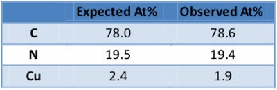
The initial stage of the profile shows the removal of hydrocarbon contamination from the surface of the device. It is very common for a few nanometers of adventitious carbon contamination to be present at the surface, which typically accumulates from exposure to the atmosphere; in fact, another key application of the MAGCIS source is the ability to easily remove contamination from samples without damaging the underlying material of interest. Comparison spectra from Figure 2 show that the acquired C1s spectrum looks identical to the reference spectrum of CuPc, indicating that the layer chemistry is as expected, and that the ion beam is not modifying the surface. The measured composition of the layer confirms it to be CuPC, as displayed in Table 1. To show how the XPS data reflects the sample chemistry, the spectrum was deconvoluted by peak fitting. The red peak in Figure 2 corresponds to the six-membered ring carbon atoms, while the blue peak reflects the carbon atoms bonded to nitrogen in the five-membered rings; green peaks arise from a complex set of loss features due to the aromatic ring systems. Preservation of these loss features indicates that minimal damage was caused by the cluster ion beam.
 Figure 2 – C1s spectrum after cluster ion etching.
After the CuPc layer is removed, MAGCIS is switched, in seconds, to monatomic mode, and the remaining device is profiled. A profile of the entire device stack is created, permitting the composition to be monitored and compared with other devices or batches (Figure 3).
 Figure 3 – MAGCIS profile of organic FET.
Analysis of biomaterials
Multi-layer organic structures are also used in the development of biosensors. Here, multi-layers of amino acids are employed to create the surface to attach the sensing ligands, controlling the ease and stability of attachment, packing density of the ligands and efficiency of the sensing system. One example is a surface plasmon resonance (SPR) biosensor, which is used to detect the presence of particular proteins by changes in the optical properties of the sensor when the target molecules attach to the binding surface of the device. Understanding the production of the amino acid multi-layer substrate is an important step in the development of a working sensor.
Alternating layers of two amino acids—phenylalanine (Phe) and tyrosine (Tyr)—make up the multi-layer (Figure 4). These layers are made by thermal evaporation of the solid materials onto a silicon substrate. The two molecules are similar, differing in the additional hydroxyl (–OH) only. This subtle change is easy to detect by XPS, as shown in the reference spectra of the two samples. The presence of the Tyr layers can be observed by a change in the oxygen quantification and in the intensities of the components of the C1s spectrum. During profiling, the integrity of the amino acid can be monitored by the presence of what is known as a “shake-up” feature, characteristic in this case of the presence of the aromatic ring in both molecules. Any sputtering damage to the sample will cause this feature to disappear, as shown in Figure 5. If this feature disappears when using the cluster sputtering source, then it is due to the sample and not the experimental method, unlike monatomic ion bombardment.
 Figure 4 – Structures and C1s spectra of phenylalanine and tyrosine.
 Figure 5 – C1s spectra from monatomic Ar+ profile of amino acid layers showing damage to the molecule.
Figure 6 depicts the depth profiles from two samples. The first shows that the top Phe layer has been damaged or incorrectly deposited, and is much thinner than expected. Their oxygen signatures allow the three Tyr layers to be identified easily, and the layers appear to be deposited correctly. The second profile shows that the expected structure was deposited. Cluster ion profiling’s ability to analyze these kinds of materials makes it possible to fully comprehend the structures being made, and potentially make increasingly complex modifications to customize devices for specific uses.
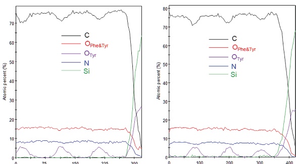
Figure 6 – MAGCIS cluster profile of (a) damaged and (b) intact amino acid multi-layer.
Summary
Since their recent introduction to surface analysis, gas cluster ion sources have become a standard addition to XPS systems. Their ability to remove material from the surface while preserving the underlying chemistry is unmatched by previously available technology and has permitted the analysis of samples that could not be analyzed successfully. Combining this with a more traditional monatomic ion source like the Thermo Scientific MAGCIS system enables investigation of the widest possible range of materials.
Tim Nunney is surface analysis product manager, Thermo Fisher Scientific, Birches Industrial Estate, East Grinstead RH19 1UB, U.K.; tel.: +44 (0)1342 310290; e-mail: [email protected] ; www.xps-simplified.com. The author thanks Dietrich R.T. Zahn, Daniel Lehmann and Iulia Korodi from Chemnitz University of Technology, Germany, for use of the organic FET sample, and Jean-Jacques Pireaux and Pierre Louette from Laboratoire Interdisciplinaire de Spectroscopie Electronique, Facultés Universitaires Notre Dame de la Paix, Namur, Belgium, for the use of the biosensor multi-layer sample.