The ability to control the size and shape of deposited chemical structures on the nanoscale opens up new and exciting possibilities for the development of devices for use in the electronic, life science, and medical diagnostic fields.
Dip Pen Nanolithography® (DPN®, NanoInk Inc., Skokie, IL) is a nanofabrication technique that combines the high resolution of atomic force microscopy with the ability to deposit both hard and soft materials. While there are a variety of techniques that can be used for generating nanostructures on surfaces, few can challenge the ability of DPN to work with a toolbox of materials ranging from metals to biological compounds such as peptides, proteins, and DNA.
The ability to work with such a large toolbox enables the construction of biological nanoarrays, rather than microarrays, allowing researchers to explore single-particle binding and positioning events. Because DPN can manipulate individual nanostructures within an integrated device or material, it is possible to fabricate biological chips, combinatorial chemical templates, and important tools for the semiconductor industry.
The technique uses an atomic force microscope tip to deposit materials on a surface and permits controllable direct-write “constructive” nanopatterning with a broad range of “inks,” including so-called “soft” biological material such as DNA, proteins, and peptides.
History and development
In 1989, Dr. Don Eigler of the IBM Almaden Research Center (Armonk, NY) used a low-temperature, ultrahigh-vacuum scanning tunneling microscope (STM) to write the letters I-B-M on a nickel surface with 35 individual xenon atoms. This work was followed by the discovery that atomic force microscopes (AFMs) could also be used to organize materials on surfaces in a similar manner, but under milder conditions.
In 1999, Prof. Chad Mirkin and co-workers developed DPN at Northwestern University (Evanston, IL), perfecting the deposition of 16-mercaptohecadecanoic acid (MHA) on gold surfaces. The group found that the technique could be used to deposit controlled amounts of material at specific points on a surface, and was versatile enough to be used as a flexible nanoscale patterning tool for template-directed assembly and biological material deposition.
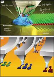
Figure 1 - a) Schematic of DPN process. A molecule-coated single AFM tip deposits ink via a water meniscus onto a substrate. (Reproduced with permission from Ref. 1.) b) Schematic representation of DPN process scaled up for massively parallel nanopatterning. The figure depicts the ultimate aim of rapidly creating a variety of structures on the fly, with different inks on each tip.
Since then, DPN has evolved from a single- ink, single-tip research technique to a multiink, multitip surface patterning technique. In some cases, it is capable of exceeding the throughput of electron-beam (e-beam) lithography, which can pattern between 10 and 10,000 μm2 in an hour.
For the majority of inks, the DPN transport process is understood to be mediated by the water meniscus that forms between the inked AFM tip and the substrate due to capillary condensation. The ink molecules transfer from the tip to the substrate when the tip is either drawn across the substrate or kept in contact with it (see Figure 1a and b).
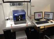
Figure 2 - NSCRIPTOR desktop DPN instrument.
In order to enhance the versatility and ease of use of DPN, a suite of tools has been developed that includes microelectromechanical systems (MEMS) devices; software; and most notably a dedicated lithography instrument, the NSCRIPTOR™ (NanoInk) (see Figure 2). The NSCRIPTOR DPN instrument can be used to deposit materials with line widths as thin as 14 nm and with feature placement precision greater than 10 nm. It is capable of both bottom-up (e.g., self-assembly, templating) and top-down nanofabrication.
The 55,000-tip 2-D nano PrintArray™ DPN (NanoInk) overcomes the inherently serial nature of DPN, enabling massively parallel nanopatterning suitable for high-throughput nanofabrication.
Table 1 - Comparison of nanopatterning techniques
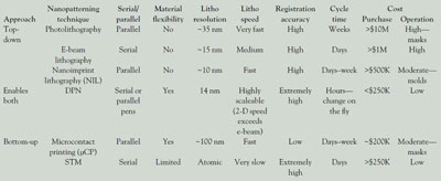
Table 1 provides an overview of nanopatterning techniques. Among sub-50-nm techniques, such as e-beam lithography, only DPN can directly deposit molecules under ambient conditions. In addition, because NSCRIPTOR is based on SPM technology, it is capable of pattern fabrication and immediate verification of the result by AFM imaging. This is frequently important, since current drawbacks of the DPN technique often relate to ink transport and overall process control. Rather than replace the techniques shown in Table 1, DPN is poised to complement them, since its attributes make it an effective nanopatterning method.
Ink delivery systems
The process of inking a DPN pen can be as simple as dipping it in a vial with a pair of tweezers. However, when using the technique to create specific structures for devices, repeatability and process control are critical.
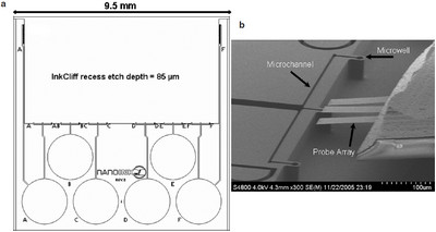
Figure 3 - a) Top view schematic of a Universal Inkwell. b) Array of three cantilevers dipping into the microplate of a Universal Inkwell. The ink is selectively delivered only to the intended center tip, and cross-contamination is prevented by etch-isolation.
To ensure overall process control, ink must be delivered selectively from uniformly loaded cantilevers with no cross-contamination. To ensure this, Universal Inkwells™ and DNA Inkwells have been developed (NanoInk) (Figure 3) that enable controllable inking by aligning microfluidic channels precisely with the cantilever arrays. The design accommodates a variety of active and passive pens, and incorporates etch-isolated microplates that protrude from the surrounding chip, providing an inking peninsula that isolates the ink-dipping event and prevents wicking or contamination. Current designs include microplates that are fed by six reservoirs, which can contain six different inks.
The inkwell design provides isolation, containment, and optimized fluid flow (to the microplate) while enabling accurate control of cantilever ink loading—an important factor for inks that must be deposited with their native solvent (e.g., DNA, proteins, and/or metal nanoparticle-based inks).
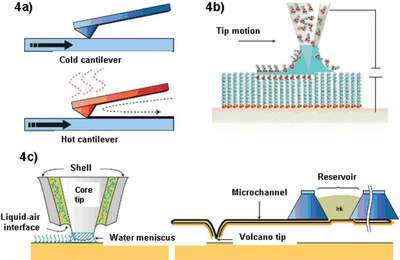
Figure 4 - Depiction of nanofountain pen lithography concept. (Reproduced with permission from Ref. 1.)
Another way of controlling the inking process is to use a nanopipet “volcano”- like tip design to create a nanofountain pen lithography system (Figure 4). This approach relies on ink from microchannels linked to ink reservoirs for steady ink flow, as opposed to coating the tip itself. While many find it necessary to have tips with holes and a steady supply of liquid ink, this turns out to be unnecessary in the majority of patterning situations, since the amount of ink stored on the tip is more than adequate for many continuous hours of writing.