The helium ion microscope is being proven to offer solutions for imaging at the nanoscale. The high brightness of its ion source gives the microscope a subnanometer probe size. There are also unique features to the beam–sample interactions that produce the image information, thus allowing for new data to be gleaned from the images. Some fundamental advantages conferred by probing a surface with a helium ion beam are the unique and complementary material dependence of the secondary electron (SE) yield, the surface sensitivity arising from the small SE escape depth, and the ability to maintain this surface sensitivity even when imaging low-atomic-weight materials—thus eliminating the need to decrease the beam energy (degrading resolution) in order to see the true surface. Since the helium ions have such low mass, sample damage is greatly reduced, allowing focused ion beam (FIB)-specific applications to be carried to a much higher magnification. At the same time, this low mass makes it possible to collect the backscattered ion signal to create a new imaging mode. Insulating samples can be managed through the use of an electron flood gun to neutralize charge buildup. Finally, there is a large depth of focus in the microscope, allowing highly three-dimensional objects or slanted surfaces to be imaged more readily with uniform clarity across the field of view.
The ORION™ helium ion microscope (Carl Zeiss SMT, Peabody, MA) is a new entry in the field of charged particle optics. The ion source is based on the field ion microscope developed by Müller in the 1950s.1 Several workers have since created and characterized gas field ion emitters in various embodiments.2 However, the challenge in commercializing such a technology has been in obtaining a reproducible emitter with sufficient lifetime. Ward et al.3 overcame this problem, and their efforts resulted in the development of the ORION helium ion microscope. The benefits of a gas field emitter are the atomic-sized source (atomic level ion source, ALIS) afforded by the principles of field ion emission and the ability to run noble gases, avoiding the use of contaminating metal ions as in the liquid metal ion source. In addition, the ability to use low-mass helium ions dramatically reduces the sample damage created by sputtering. Diffraction effects, which limit the ultimate spot size of an electron beam, become irrelevant since the helium ion beam has 1/86 the wavelength of an electron beam of equal energy.
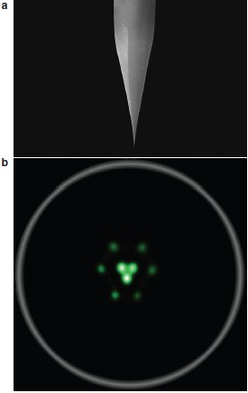
Figure 1 - a) ALIS tip, b) field emission pattern from the ALIS.
The ALIS consists of a sharp metal tip (Figure 1a) cooled to cryogenic temperature and held at a high positive potential. Helium gas introduced into the region of the tip, after being adsorbed onto its surface by the combined action of low temperature and high field, is ionized at the electric field maximum that is found over each atomic center. The resulting ion beam from each atomic-sized emitter is utilized as the source. The key to ALIS technology is a formation process that produces a special structure on the end of the tip, reducing the emission sites from the hundreds normally visible in the field ion microscope (see Figure 1b) to a very small number, only three of which carry most of the ion current. The microscope’s ion gun allows for one emitter from this group to be selected for transmission through the electrostatic ion optics, yielding a single, stable ion beam with high brightness (>5.0 × 10⁹ A-cm–2-sr–1). A probe size of 0.25 nm is predicted with the current optics; thus far measurements have achieved ~0.5 nm. The interested reader may see Ref. 4 for further information.
Imaging and applications
While the image is created by the same method as a scanning electron microscope (SEM), the uniqueness of the tool lies in the contrast mechanisms, which are partially like an FIB, partially SEM-like, and having qualities also specific to helium ions. This, combined with the microscope’s high spatial resolution, leads to an exploration of applications in nanoscience imaging. This paper presents a discussion of several of these, illustrated by examples that highlight what can be achieved.
Interaction volume
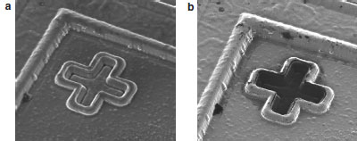
Figure 2 - Semiconductor sample highlighting the material contrast in SE images produced with the helium ion beam: a) SEM image, b) helium ion microscope image.
While the resolution of a microscope is often quoted as its probe size, the true image resolution is a convolution of this value and the interaction volume of the probe with the sample, that is, the lateral extent of the volume from which secondary particles are emitted may be larger than the incoming probe size. This degrades resolution and contrast. Also, particles arising from deeper regions of the surface can degrade the true surface information in the signal. For an electron beam, a significant portion of the signal can consist of type-II SEs, which arise from the backscattered electrons as they exit the sample.5 There is no such contribution from a primary ion beam. Further, we find that the secondary electron yield induced by an ion beam varies with material over a range of about 3–10. This is higher than for an SEM. This provides the helium ion microscope with greater signal at a given beam current and greater material contrast. Figure 2 shows an example of this, comparing the SE image from a conventional SEM (Figure 2a) to a helium ion microscope (Figure 2b). Both images show surface topology, but the helium ion image displays two features in addition. The first is the richer material contrast, as compared to the more constrained gray scale of the SEM image. The second is the crisper surface information in the image. This is discussed further below.
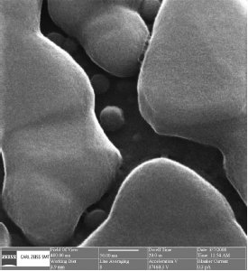
Figure 3 - High-resolution image of gold particles on carbon highlighting the surface detail and sharp edge definition. The probe size of the helium beam calculated from this image was 0.54 nm.
The secondary electron spectrum from an incident helium ion beam peaks below 5 eV and falls off quickly. The escape depth from the sample for such low-energy electrons is just a few nanometers; thus these electrons all provide an image of the very near surface. The backscattered ions can produce type-II SEs, but these are small in number since the backscatter yield is below 10% for most materials and the backscatters themselves, being of lower energy, release fewer SEs than the primary beam does. The surface quality of the images can be seen more readily in high-magnification images, such as the example presented in Figure 3. In this helium ion micrograph of evaporated gold particles, we see excellent edge definition of the particles and also fine surface detail on the top of the particles. This is evidence of the surface sensitivity explained above. It is a unique offering of the helium ion microscope that surface sensitivity can be achieved simultaneously with the smallest probe size, i.e., the highest beam energy.
Surface contrast
Figure 4 - NBPT double layer over a gold film, patterned with an e-beam mask: a) SEM image, b) helium ion microscope image.
Related to this concept of reduced signal generation volume is the ability to image thin surface layers and surface chemical states. An example of this is seen in Figure 4, which shows a nitrobiphenyl-thiol (NBPT) patterned monolayer. Electron beam patterning via a stencil mask was used to reduce the terminal nitrate group at the surface to an amine group. Thus, the contrast in the image must be provided solely by this substitution of oxygen by hydrogen at the top chemical unit of the surface. Whereas the SEM image in Figure 4a only shows a faint outline indicating that some change in the surface has occurred, the helium ion micrograph in Figure 4b shows clear chemical contrast from the amine terminated areas.
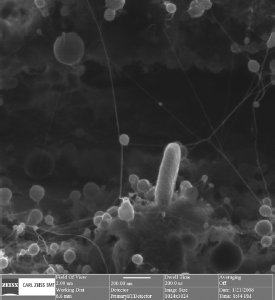
Figure 5 - Single-wall carbon nanotubes suspended above a silicon surface on SiGe catalyst particles; 70° tilt of sample from beam axis.
This ability can also be leveraged into many other applications that require imaging low-atomic-weight materials. Figure 5 shows an image of single-walled carbon nanotubes. These can be imaged at high beam energy without becoming transparent to the beam. SEM imaging of these requires low beam energy to avoid this problem.