Most microscopists are familiar with confocal microscopy from neuroscience or cell biology. However, very quietly and abruptly, confocal has jumped the fence into industry, becoming a major tool-of-choice for measuring surface texture and wear as well as evaluating thin film thickness and counting, sizing, and defining distribution of particles in epitaxial films.
Twenty years ago, when confocals first became commercially available, white light confocals were rare. LaserTec (San Jose, CA) and the K series from Technical Instruments of San Francisco (TISF, now Hyphenated-Systems, Inc., Burlingame, CA), were the only real competitors. Today, the field is crowded and highly competitive. Recent estimates by The Microscopy & Imaging Place, Inc. (McKinney, TX) put the market for this version of confocal microscopy at about $80 million/year, with a projected growth rate of 20% per year each year for the next three years.1
As with conventional biological confocal microscopy, industrial confocals scan the specimen surface with a pinpoint of light, then, at the detector, limit the diameter of the resulting image forming beam. As seen in Figure 1a, the resulting image has shallow, well-defined depth of field and an image free of haze and glare. Scanning the stage in the Z direction produces a series of these well-defined planes (Figure 1a–e), which can then be combined in software to create 3-D reconstructions (1f).
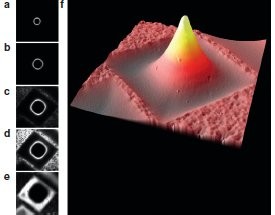
Figure 1 - a–e) A series of confocal sections acquired at defined Z locations moving from the top of the structure to the bottom. (f) The resulting 3-D reconstruction. (Images courtesy of Leica GmbH, Wetzlar, Germany.)
Biological confocals often use lasers as the light source and scanning mirrors to scan and descan incoming and resulting sample beams. Initially, industrial confocals primarily used white light sources and acoustic-optical tunable filters or spinning disks with arrays of pinholes or slits to scan and descan the beam. Also, while most biological confocal systems use fluorescence to generate images, their industrial cousins use reflected light.
Today, industrial confocals span both the laser scanning and white light spectrum. Keyence’s VK-9700 (Woodcliff Lake, NJ) and Olympus Industrial’s LEXT 4000 (Center Valley, PA) use a white light source for true-color confocal imaging and a violet light-emitting diode (LED) as a secondary light source to enhance resolution. As seen in the equation below*, to calculate the Rayleigh limit of resolution, resolution is directly related to wavelength: Shorter wavelengths enhance the imaging of finer detail. Carl Zeiss (Thornwood, NY) offers two versions of confocal: the more industrial ASM 700, which is a white light system, and the more traditional laser-based LSM 700. While the ASM 700 operates in reflected light mode used in most industrial applications, the LSM 700 offers a combination of both fluorescence and reflected light mode, making it an interesting solution in situations in which fluorescence can be applied to image and measure defects, contamination, or special particles of interest.
*Resolution = 0.6l/NA, where l is the wavelength of light, and NA is the numerical aperture related to the collecting angle of the objective.
Two- and three-dimensional parameters describe complex structure:function relationships
The world of surfaces is a complex domain. Characterizing surfaces is critical. The way a surface behaves, wears, or changes over time or in the presence of a specific environment determines how the things around us function, whether it is the polymeric coating that maintains crispness in a bag of potato chips or the smooth ball bearing that keeps airplanes aloft.
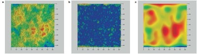
Figure 2 - Ceramic floor tile: a) Composite image of surface texture, b) roughness component, and c) underlying waviness. Each image was taken with an EC Epiplan Neofluar® (Carl Zeiss), 10×/0.25. Single plane: 4163.9 µm × 4163.9 µm × 159.0 µm. Image size: 1024 × 1024 pixels × 54 planes. (Image courtesy of Carl Zeiss, Inc.)
For decades, surfaces have been described in terms of 2-D roughness parameters such as average roughness, peak-to-valley ratios, and peak heights. However, underlying the 2-D characterization may be larger, 3-D influences such as waviness or bow. Both have an impact on how a surface will perform. Figure 2 illustrates the level of today’s roughness characterization. Figure 2a shows the composite roughness characterization of a ceramic tile, while Figure 2b and c depict the roughness and waviness components, respectively.
Traditional profilometry sets the standards
Table 1 - Sample comparison of roughness measurements offered by traditional white light interferometers (A) and today’s
industrial confocals (B)*
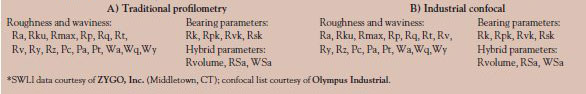
For decades, terminology in this arena has been set by more traditional stylus and scanning white light interferometers (SWLIs). As seen in Table 1, industrial confocals are catching up. The Olympus LEXT is a case in point. Its graphical user interface (GUI) has been designed to represent roughness, waviness, and bearing ratio parameters in the same terms used by conventional optical profilometry.
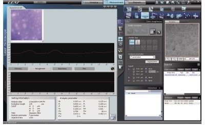
Figure 3 - The user interface for LEXT confocal mirrors a typical SWLI interface. (Image courtesy of Olympus Industrial.)
Not only are the parameters parallel, but presentation and reporting mimic stylus and SWLI formats. As shown in Figure 3, Olympus has designed a special GUI to replicate a profilometer menu, including all ISO parameters. In addition is the ability to filter the data to match a profilometer for correlation.
Piecing together the world at large
Unlike interferometry, the field of view (FOV) in confocal microscopy is determined by magnification of the objective. In the simplest terms,
FOV = FNep/Mobj
where FN = field number of the eyepiece and M = magnification of the objective. As magnification increases, the field of view under observation decreases. How, then, does one compute roughness parameters that are representative of the material at large? Most of the confocal companies now offer stitching programs, which, as depicted in Figure 4, combine a sequence of smaller scans into a larger whole.
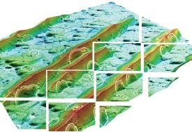
Figure 4 - Special stitching software allows
smaller areas to be combined to provide
large-area analyses. (Image courtesy of Leica.)
Stitching presents challenges both mathematically and empirically. Microscope stage movement is not always exact, requiring stitching algorithms to seek information about what was really at the edge of Plate 1 to match it properly with some similar fiduciary structure at the edge of the adjoining plate. Moving from 2-D to 3-D makes the process even more challenging. In its Zen software, Carl Zeiss has instituted next-generation stitching that not only matches segments in XY, but also in Z.
Who’s doing what?
Industrial confocals are offered in a variety of configurations and capabilities. Generally, they fall into two categories: more traditional configurations versus hybrids. The Zeiss ASM 700, Keyence VK-9700 series, and Olympus LEXT all fit neatly into the more traditional mold. Each has unique tweaks, but as a group, they offer ease of use, excellent 3-D imaging, and a wide range of surface metrology capabilities. Hyphenated-Systems (now distributed as the Bruker AXS [Tucson, AZ] VCM™ confocal microscope) is also a member of this cadre, but differs somewhat in its advanced 3-D reconstruction capabilities.
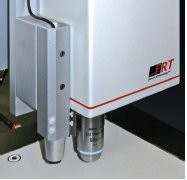
Figure 5 - FRT’s open architecture combines field-of-view confocal microscopy (right
objective) with a chromatic white light confocal point sensor (left) for large area raster scans.
Among the hybrids, each group member is radically different. As shown in Figure 5, the open architecture in the MicroProf 200®(FRT, San Jose, CA) architecture allows the user to configure the microscope to fit the measurement need. In this case, the right objective provides an optical path for conventional field-of-view confocal microscopy. The left “objective” is actually a chromatic white light confocal point sensor for large area raster scan measurement. This system can also be extended to include SWLI and atomic force microscopy (AFM), all on a variety of stages ranging from conventional microscope format to very large gantry formats.
Leica is now offering a customized version of Sensofar’s (Barcelona, Spain) dual core system as the DCM 3D Measuring microscope, combining interferometry and confocal on one stand. This combination is intriguing in that it offers phase shifting and white light interferometry for characterization of very smooth surfaces (<1 nm in roughness) with confocal’s higher XY resolution. Leica has extensive experience in bullet analysis, and this new offering presents another important tool in that arsenal.