Thin polymeric films and surfaces provide novel electrochemical, thermal, mechanical, and/or biocompatible features at the nanoscale level in the development of adhesives, protective coatings, lubricants, and suspension stabilizers, as well as in semiconductor devices such as biosensors used in medicine.
The interface between the film and substrate principally determines the structural and thermodynamic stability of multiphase polymer systems, and the interface between the film and external environment determines the specialized functionality of the film. A comprehensive understanding of the thermodynamics at the nanoscale level is crucial to the development of better manufacturing practices that strengthen film–substrate interfaces and accentuate the functionality of film–environment interfaces.
High-resolution electrical impedance spectral studies on silicon
Silicon wafers provide surfaces that are suitably flat at the atomic level for dielectric spectral (DS) characterizations of the structural and topographical features of nanostructures. Figure 1 illustrates the dielectric spectrometer and details the characterization chamber (Inphaze Pty. Ltd., Sydney, Australia), into which functionalized surfaces are mounted. The system’s design3 ensures a uniform density of the alternating current stimulus, i, that enables full utilization of the 24-bit acquisition of the response, v, and yields better than one-thousandth of a degree resolution in phase at frequencies as low as one-thousandth of a Hertz.4 Angstrom resolutions have been achieved with the Inphaze technology on silicon2 and gold.1
Theoretical background
Dielectric characterization is broadly based on the degree to which the electrical properties of a nanostructure of dielectric constant, εr, and thickness, d, depart from those of an ideal parallel plate capacitor, the capacitance (per area) of which is given by:
where εo is the dielectric permittivity of free space (= 8.85 10–2 Fm–1). Real capacitors leak electric charge with a characteristic time constant given by:
where g denotes the leak conductance, which is 0 for an ideal capacitor. The reciprocal time constant yields a characteristic frequency given by:
below which the electrical properties are dominated by the leak conductance.
Dielectric characterization of a monolayer and bilayer
Figure 2a shows the measured capacitance of an octadecane monolayer on a highly conducting atomically flat silicon substrate in contact with a 100 mM KCl electrolyte. The fitted curve was generated using the shown values for the parallel plate capacitor, c2, the leak conductance, g2, and the series conductance, g1, representing the electrolyte. The value for c2 is given by those measurements below 200 Hz that are characterized by the frequency independence predicted by Eq. (1). Equations (1) and (3) yield estimates of the thickness d2 (assuming εr = 2.05) and the frequency constant that were consistent with those expected for the monolayer,2 and are represented in the structural line-spectrum shown in Figure 2c as a step in thickness at this frequency constant value.
Figure 2b reveals the manifestation of a second constant capacitive regime in the frequency range of 10–103 Hz after vesicles of phosphatidylcholine:cholesterol (2:1 mol/mol) were placed onto the monolayer. This manifestation is accommodated in the model for the monolayer alone by the series addition of an ideal capacitor, c3, and its leak conductance, g3, which is consistent with the vesicles adsorbing to the octadecane surface to form a second monolayer. Figure 2c shows that the structural line-spectrum for the bilayer  contains two steps. The step characterized by the lowest frequency constant is very similar in height and location to the step obtained for the octadecane monolayer alone
  , indicating that it characterizes the thickness (assuming εr = 2.05) and frequency constant for the base leaflet of the bilayer comprising octadecane. Thus, the second step characterized by a frequency constant value that is two orders of magnitude greater than that of the monolayer characterizes the phosphatidylcholine:cholesterol upper leaflet.
Dielectric characterization of native silicon oxide surfaces
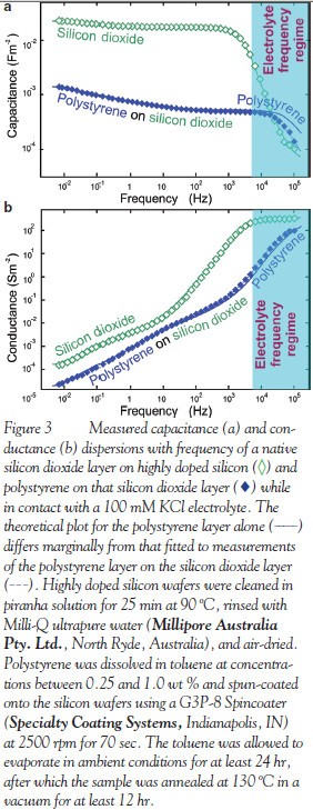
Figure 3a shows that capacitance measurements for a silicon dioxide “layer”  disperse continuously with frequency over the frequency range at which distinctive plateaus in capacitance dispersions shown in Figure 2 previously identified the presence of two electrically specific layers. The continuous dispersion is that expected for several electrically distinct sublayers. This is consistent with extensive studies reviewed by Grunthaner and Grunthaner7 involving a variety of techniques including X-ray photoelectron spectroscopy (XPS), nuclear magnetic resonance (NMR), contact angle measurements, ellipsometry, and surface extended X-ray absorption fine structure (SEXAFS). These studies show that the silicon dioxide layer indeed comprises five to six sublayers in which SiO4 tetrahedrons bridged by the oxygen atoms form regular ringed cages comprising four tetrahedrons approx. 4.3 Å in size next to the Si(111)/SiO2 interface, transitioning to eight tetrahedrons approx. 7.8 Å in size at the SiO2 surface. The dielectric characterization identified these sublayers, as illustrated in the structural line-spectrum
  shown in Figure 4, in which the steps have been reordered such that thickness values of layers (assuming εr = 4.4) increase toward the surface in concert with cage size.
The dielectric characterization further reveals that the frequency constant values taper away from the value attributed to the Si(111)/SiO2 interface, consistent with the density of sites where silicon interacts with dopant to promote electrical conduction, decreasing with increasing cage size. The sharp increase in the value for the sublayer at the surface is consistent with the permeation of highly conducting electrolyte into the voids of the SiO2 cages increasing with increasing cage size.
Dielectric characterization of polystyrene on silicon dioxide
Figure 3 further shows an order of magnitude decrease in the measured capacitance and conductance after a polystyrene film was spun-coated onto the SiO2 surface. It additionally illustrates an increase in the extensiveness of the capacitance dispersion expected from the addition of further layers. These differences are more precisely reflected in Figure 4, which reveals a structural line-spectrum for polystyrene that features more steps than that for silicon dioxide , which in turn features more steps than those spectra shown in Figure 2c for the bilayer , which features two steps, and the monolayer , which features only one step.