Much of the innovative
activity in scanning electron microscopes (SEMs) has been devoted to ultrahigh-magnification instruments for
the use of researchers characterizing
materials and processes at nanometer
scales, but there is also a growing interest
in robust industrial tools operating
at more modest magnifications.
Industrial applications often require
throughput rates that would be impractical
for traditional manually operated
instruments; in an ever-evolving
workplace, companies are also increasingly
relying on engineers and technicians
to collect the needed data in
close proximity to the process being
monitored, rather than the services
of professional microscopists working
from a central laboratory. The need
for large quantities of quality data as
quickly and consistently as possible is
driving new expectations for reliability
and automation—an emphasis that is
encouraging an integrated solution-driven
approach to SEM technology.
This new approach represents a different
way of thinking about SEM performance,
and has fostered a “system”
approach to SEM design.
Technologies and
techniques
A system approach to automated microscopy implies that all aspects of
the instrument are optimized for the efficient
performance of the specific task(s)
to be addressed. Whereas instruments
designed for research applications are
typically characterized by technical performance
specifications, such as attainable
resolution, a solution-driven tool
is most meaningfully characterized in
terms of its ability to assess key specimen
metrics with the necessary speed
and precision. In order to optimize this,
all components of the system (including
both hardware and software) must function
together as an integrated whole.
Use of dynamic beam control to
optimize data collection
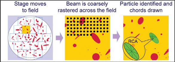
Figure 1 - Dynamic beam control for scanning samples. Minimal
time is spent on “empty” pixels by dynamically analyzing the
specimen.
A key technology for efficient automation
is dynamic beam control. The basic idea is
to spend as little time as possible collecting
pixels that have no relevancy to the problem.
To accomplish this, a “smart” beam control
algorithm is employed (Figure 1) wherein the
beam is rapidly stepped across the specimen
using a relatively coarse raster that will pick up
the smallest features (e.g., particles) of interest.
When an interesting feature is detected,
a sizing algorithm is initiated with a much
higher resolution and an X-ray spectrum may
be collected. Thus, features of interest can
be characterized to arbitrarily high precision
while minimizing the time spent in collecting
uninteresting pixels. This is in contrast to
the more conventional frame-based type
of computerized analysis, where a complete
frame of pixels is first measured at
the finest resolution required, and is then
analyzed by image-processing software.
Since a SEM is a sequential-pixel device,
and the vast majority of pixels in a typical
image frame are not of analytical interest,
dynamic beam control results in dramatic
improvements in measurement speed.
Data→information→knowledge
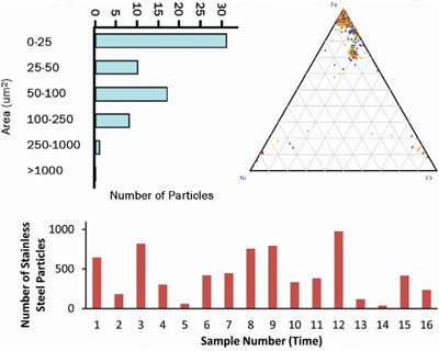
Figure 2 - Automated reporting output for wear debris
analysis. Size distribution histogram can be vital to understanding
the type of wear mechanisms that can occur in a system
(a). A ternary phase diagram of steel particles illustrates
the difference between different alloys of steel (b). Finally, the
automated trending capabilities provide investigators with the
ability to easily monitor changes in the process through control
charts (c).
Rapid collection of data is important,
but perhaps more important is turning
those data into application-relevant
information and knowledge. An automated
instrument can easily produce a
deluge of data that would be overwhelming
without the aid of appropriate report-generating
software that consolidates the
measurements into readily interpreted
metrics and trends. Ideally, such reporting
software is further structured with
knowledge of the particular kind of
application so that the reports express
the metrics most important to the industry
or application being served. If we take
a wear debris application as an example
(Figure 2), material wear is fundamental
to understanding how a system performs
over time. Consequently, the knowledge
gained from the data is not in the individual
data points but in the distribution
of particle sizes and shapes and the pattern
of change over time.
Addressing the X-ray bottleneck
Due to steady improvements in refining
the dynamic beam technique, it can now
be demonstrated that a random mixed field
of circular features can be identified and
measured at a rate of 600/min with a size
precision of better than 50 nm. Impressive
though this may be, until recently the hard
reality was that, when it was necessary to
assess elemental composition, the collection
of an X-ray spectrum required a few seconds per particle, which thus becomes the critical limitation for
analysis throughput in most practical applications.
A technology breakthrough in the measurement of X-rays first surfaced
approximately 10 years ago as the new technology of silicon drift detectors (SDDs) began to replace the venerable lithium-drifted silicon
detector. Not only did the new SDD technology eliminate the requirement
for liquid nitrogen cooling, but excellent energy resolution could
be sustained at much higher counting rates. However, to translate this capability into higher throughput, it is necessary to deliver more X-rays
to the detector. To some degree, this can be addressed by using higher
beam currents, but since this also means larger beam diameter, spatial
resolution is eventually compromised. Thus, increased emphasis is now
directed toward increasing the collection efficiency of the detector
itself. Two viable strategies are the use of larger detectors and multiple
detectors, and though these are indeed effective approaches, they also
have a substantial cost impact (as well as other practical limitations).
Integrating the X-ray detector for optimal performance
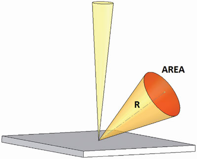
Figure 3 - Maximizing omega to improve collection efficiencies of X-ray detectors.
If the detector is represented by a circular surface area, located a distance R
from the point where the beam impacts the specimen, then the solid angle (omega)
is expressed as the area divided by the square of the distance (R). Ω = area/R2.
The most cost-effective means of improving detection efficiency is
to place the X-ray sensor as close as possible to the point where the
X-rays originate from the specimen (Figure 3). In practice, however,
such optimization has traditionally been circumscribed by the conventional
construction of the X-ray detector, in which the active sensor element is located at the end of a long tube that it is inserted
through a port in the microscope chamber. Though this modular
tube mount configuration has served the industry well for decades,
it has also restricted how closely and flexibly the sensor element
can be positioned relative to the specimen. This limitation has
recently been addressed by the introduction of the OmegaMax™
technology (patents pending, ASPEX, Delmont, PA) in which the
SDD sensor is built directly into the structure of the microscope.
This has permitted the effective solid angle (omega) of the detector
to be increased by several multiples over what had been achieved
with conventional tube-mount detectors.
In fact, the improvement in detection efficiency is so dramatic that
smaller-area sensors can be employed that
still deliver substantially enhanced detection
efficiency, but with the additional
benefit of improved energy resolution, and
all without an increase in cost to the user.
This dramatic advance was made possible
by considering the X-ray detector not as a
separate entity, but as an integrated component
of a system whose objective is to
provide practical industrial solutions.