Micro X-ray fluorescence (MXRF) is a
powerful elemental technique that
can nondestructively provide both
single-point spectra and full spectral
elemental maps.1 The X-ray spot size
of a commercial instrument is approx.
10-50 μm; thus, an elemental map
may contain between 1600 and
40,000 pixels. Full spectral mapping of
the sample can therefore generate the
same number of discrete spectra.
MXRF images are important because
they provide several orders of information,
including qualitative and quantitative
information on elemental
species, as well as heterogeneities and
spatial distribution of the elemental
species present. The mapping capability
essentially provides a picture of the
elemental distribution within the
material, which very easily provides a
tremendous amount of information.
Collecting full spectra at each pixel
generates hyperspectral data sets.
When these hyperspectral data sets
are processed with chemometric software,
unexpected elements may be
detected and chemical phases
revealed (i.e., elemental correlations
are spatially identified).2 The typical MXRF instrument uses an optic to
spatially restrict the excitation X-rays
to a small spot, with no optic on the
detector. Therefore, fluorescent X-ray
photons are detected from the full
critical depth of the analyte excitation.
Elemental discrimination as a
function of depth is not possible in
this approach.
Confocal X-ray fluorescence uses an
optic on both the excitation source and
the detector. This arrangement produces
the confocal volume, allowing
one to spatially discriminate the source
of the X-ray fluorescent photon in both
the x–y directions as well as the z direction.
A schematic layout of a typical
confocal MXRF is given in Ref.
3. A more recent demonstration
of a laboratory confocal system
has been published.4 Confocal
MXRF has also been previously
discussed using a synchrotron5;
however, synchrotron availability
is limited. The current confocal
instrument fits easily on a
24 × 24 in. breadboard, with the
associated electronics on a rack
underneath and the computer
workstation next to it. The
small size of the instrument
makes it ideal for on-line, at-line,
and off-line measurements.
Confocal MXRF can be used in
such applications as forensics,
cultural provenance, minerals,
materials sciences, thin films,
particulate characterization,
pharmaceuticals, polymers,
fossils, nanotechnology, and
many others.
Instrument design
An X-beam Ag X-ray tube (X-ray
Optical Systems [XOS] East
Greenbush, NY) powered by an XLG
high-voltage power supply (Spellman
High Voltage Co., Hauppauge, NY), 50
kV, 0.5 mA, 25 W max, was used as the
X-ray source. A Si pin diode detector
(model XR-100CR, Amptek, Bedford,
MA) was used to detect the X-ray fluorescent
photons. The source and detector
optics consisted of a pair of monolithic
polycapillaries (XOS) with a focal
spot size of approx. 35 μm. The angle
between the optics is approx. 60°, 30°
from the surface normal of the sample,
producing a working distance of 10 mm.
This optical arrangement is a compromise
between the ideal 90° geometry for
optimum spatial resolution and greater
X-ray depth penetration into a specimen.
Three 850G actuators (Newport
Corp., Irvine, CA) were used to drive
the sample stages. Everything was under
computer control using XOS software.
Line profiles
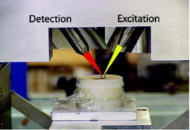
Figure 1 - Optical photograph showing tip of capillary
optics, sample position, and beam path. Sample is raised up
into confocal volume and scanned in all three dimensions.
The confocal volume was determined
by profiling a tantalum foil (10 μm
thick) in all three dimensions. The confocal
volume was found to have dimensions
of 40 μm (full width half maximum)
in the x and y directions and 60
μm in the z direction. The optics and
sample geometry are shown in Figure 1.
Each elemental signal was measured
as a function of integrated intensity under the emission band.
For each element , the line and
energy region of interest (ROI) are
as shown in Table 1.
Each element was recorded as a
function of position versus intensity.
The line profile of each elemental
intensity was normalized to
one. Dwell time was set at 1 sec,
with 30-μm spacing between measurements.
The current instrument
is limited to elements with energies
between 3 and 20 keV due to
air absorption.
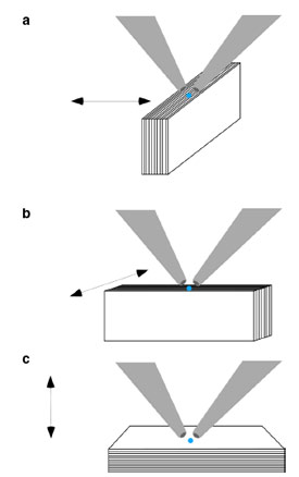
Figure 2 - Optical geometry of line scans and
3-D imaging of paint chip. Orientation A, sample
layers are perpendicular to beam; orientation B,
sample layers are parallel to beam; orientation C,
sample is laid flat. Orientation and scan directions
are offset by 90° between A and B.
The effect of sample orientation is
critical in confocal MXRF. This is
illustrated using a multilayer paint
chip. The paint chip, 1 mm thick, is
composed of calcium-, titanium-,
iron-, zinc-, and lead-based pigments.
Figure 2a–c shows the sample
orientations of the cross-
section. The paint chip appears to
have at least 18 distinct layers, with
lead more prevalent in the layers on
one side. This side will be defined
as the bottom of the sample, i.e.,
early painting.
In orientation A, shown in Figure 2a,
the sample cross-section strata are perpendicular
to the excitation–detection
alignment. The z position was determined
by the height of maximum signal;
therefore, the confocal volume
was imbedded in the surface of the
sample. The sample was then profiled
from top to bottom, which shows the
lighter elements first, followed by the
bottom lead layers. As the beam enters
the sample, it will be attenuated
slightly by the upper and
lower layers of paint.
In the second orientation
(Figure 2b), the sample
cross-section is parallel to
the excitation–detection
alignment. The line profile
was completed by moving
the sample left to right
such that the beam entering
the sample remains
approximately in the layer
being probed.
Finally, in orientation C
(Figure 2c), the sample is
laid flat and the profile is
measured by moving the
sample up through the
confocal volume. In this
instance, the upper layers will attenuate
the sampling beam and the
detection beam. In addition, the
spatial resolution is decreased by
almost 50%.
3-D imaging
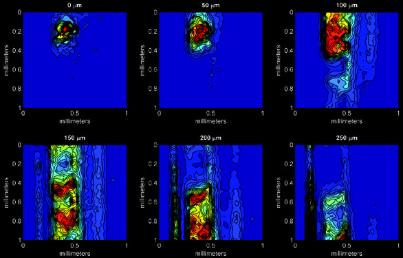
Figure 3 - Series of x–y maps at different z depths within the sample for orientation B. All dimensions
are in millimeters.
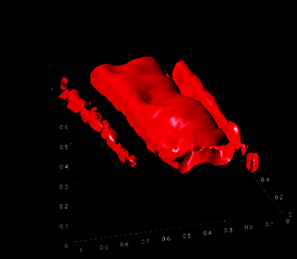
Figure 4 - Three-dimensional elemental image of titanium
from the x–y maps shown in Figure 3. All dimensions
are in millimeters.
Three-dimensional imaging is possible
because the detector optic is collecting
photons given off at the focus;
thus, a map as a function of the x, y,
and z positions versus elemental X-ray
fluorescence intensity can be collected.
As shown in Figure 3 for titanium, x–y maps at each z position are
collected successively. Importing each
of the x–y maps into MATLAB 7.04
(MathWorks, Inc., Boston, MA), it is
possible to then generate 3-D images
of each element individually, as seen
in Figure 4. In MATLAB, it is possible
to generate 2-D images, 3-D images,
and slices, as well as rotate 3-D constructs
that can be created and converted
into movies.
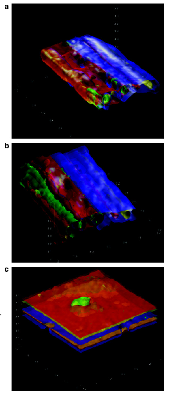
Figure 5 - Three-dimensional elemental
images of paint chip in three different orientations.
Images are rotated to have the same orientation.
Layers for A and B are up–down with respect to
the page, and are not seen to deeper depths
because of attenuation. The layers are oriented
left–right in image C. The elements are color
coded as follows: Ca = green, Ti = red, Fe = yellow,
Zn = blue, and Pb = gray. All dimensions
are in millimeters.
Full 3-D scans of the paint chip were
completed with the same orientations
as the line scans with 41 × 41
(x–y) pixel 2-D maps at 14 different
z depths. The step size per voxel is
30 × 30 × 50 μm, giving a total of
23,534 voxels, with a 1-sec dwell at
each. This produced elemental
images 1.23 × 1.23 × 0.65 mm in
size. In orientation C, only 11 z
positions were mapped due to attenuation
of the signal with depth.
Each x–y 2-D map took approx. 40
min to collect. The isosurface of
each element in the 3-D construct is
determined by the selected elemental
intensity value. Isosurfaces for
each element are 12% Ca, 16% Ti,
34% Fe, 4% Zn, and 28% Pb of their
maximum intensity. The images are
displayed as 50% transparent. These
multiple-element 3-D images are
shown in Figure 5a–c for each orientation,
respectively.
Results and discussion
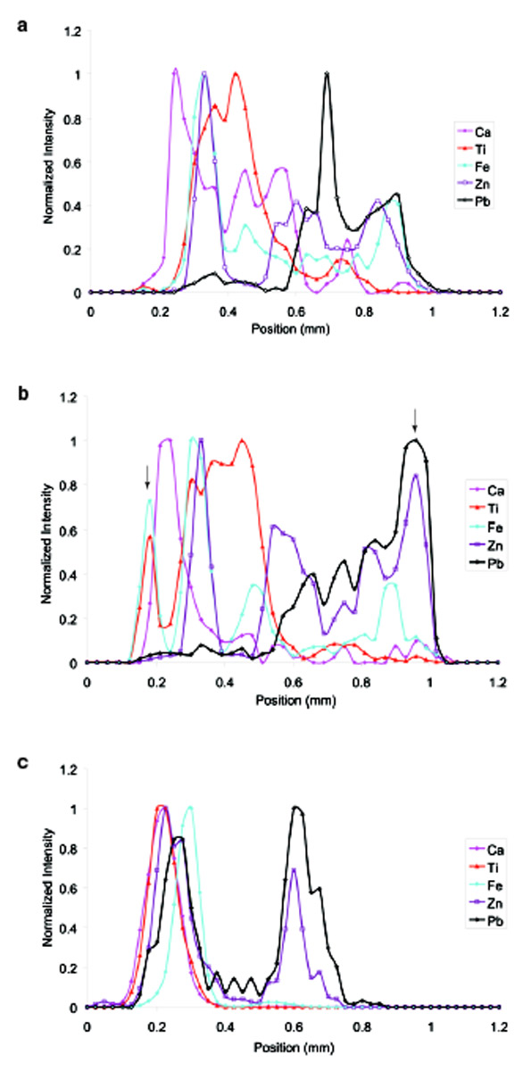
Figure 6 - Line scans of elements of normalized elemental
intensity in each of the three sample orientations shown
in Figure 2.
Comparison of the line profiles for
orientation A versus orientation B
(Figure 6a and b), shows that the
sample layers that are perpendicular
to the beam exhibit a loss in
intensity at the edges. The titanium
and iron layers are almost
completely lost on the upper surface,
and the bottom lead layer is
greatly attenuated in orientation A
(note arrows in Figure 6b). While
the two line scans comparing the
different orientations are not of the
exact same area of the sample, they
are close. Multiple line scans were
obtained in each orientation to
verify these observations.
Comparison of orientations A and B
with C (Figure 6c) produces a stark
contrast. Since the beam size in the
z direction is almost 50% larger, a
concomitant loss in spatial resolution
is seen. This loss leads to an
overlap of the layers in the individual
line scans, which are nondestructive
depth profiles. Orientations
A and B were obtained at the
cross-sectional surface while orientation
C was done in the center of
the sample. This means that both
the excitation and detection beam
will be increasingly attenuated with
depth, whereas in A and B a much
smaller portion of the beam path
was in the sample and thus experienced
less attenuation.
Figure 3 demonstrates the output of
the x–y maps from the paint chip
mapped in orientation B. Each 2-D
slice is 50 μm successively deeper into
the sample. Heterogeneities in the
titanium layer can be seen, as well as
the number of paint layers containing
titanium. As the confocal volume
probes deeper and deeper into the
sample, attenuation effects are seen,
and titanium becomes increasingly
difficult to detect, eventually disappearing
below 300 μm. Figure 4 shows
the titanium layers in 3-D after
importing the data set into MATLAB
for visualization.
Comparison of the 3-D images in
Figure 5a–c obtained in the different
orientations is also instructive.
Figure 5a shows the 3-D composite
elemental images of all the elements
mapped. While the edges appear
sharper in orientation B (Figure 5b),
as would be expected, orientation C
(Figure 5c) shows a Ca inclusion
that is not seen when the sample is
imaged on edge. This demonstrates
that the elemental distribution
information gained will vary
depending on sample orientation.
When a z depth profile is taken of a
solid single-element sample, as the
beam penetrates into the sample, an
increase will be seen in the element
intensity until the signal reaches a
maximum. The signal will then
decrease as the upper layers of the
sample attenuate the beam at greater
and greater depths, creating a null
point for the isovalue and the bottom
surface of the construct. This can be
seen in Figure 5c, where there are two
apparent surfaces for each element.
Therefore, 3-D imaging is
useful for the upper 0–400
μm of this particular sample.
The depth of penetration
will vary for each element
and its associated matrix.
Conclusion
Confocal MXRF changes the
elemental analysis paradigm
for materials characterization.
This laboratory-based
approach offers nondestructive
single-point line scans,
depth profiles, 2-D maps, and
3-D elemental images.
The current software implementation
is limited to ROI
intensities when collecting 3-
D images. Future work is
focusing on development of
enhanced software that will
collect full spectral data at
each point to utilize the
power of chemometrics for
image processing. This
enhanced software will provide
several advantages,
including reducing the scan
time, allowing for cluster
analysis in the images, as well
as postcollection processing
for elements that may not
have been noted at the beginning
of the data acquisition.
Voxel volume can also be
reduced through the use of
different capillary optics,
down to a 10-μm spot size.
Although the spatial resolution
would be increased,
scan times would also be
increased. The current 60°
angle between the optics is
not optimal. A 90° geometry would
reduce the confocal volume in the z
direction to a value comparable to
the x and y. This would improve spatial
resolution in the z direction, but
would also improve sensitivity since
the same flux would be focused into a
smaller volume, at a loss in X-ray
penetration depth.
The current data are based only on
raw signal intensity for the 3-D imaging.
Modeling of the beam attenuation on both the excitation and detection
sides is needed to provide true
elemental intensities at depth. This
would enable nondestructive, quantitative
3-D elemental imaging.
Although there is much work remaining
to make confocal MXRF a routine
method, the current capabilities show
the potential power of this method for
materials characterization.
References
- Havrilla, G.J.; Miller, T. Micro X-ray
fluorescence in materials characterization.
Powder Diffr. 2004, 19(2),
119–26.
- Miller, T; Havrilla, G.J. Elemental
imaging for pharmaceutical tablet formulation
analysis by micro X-ray fluorescence.
Powder Diffr. 2005, 20(2),
153–7.
- Ding, X.; Gao, N.; Havrilla, G. Monolithic
polycapillary X-ray optics engineered
to meet a wide range of applications.
Proceedings of SPIE—The
International Society for Optical Engineering,
2000, 4144, 174–82.
- Kanngiesser, B; Malzer, W; Reiche, I.
A new 3D micro X-ray fluorescence
analysis set-up. First archaeometric
applications. Nucl. Instrum. Meth.
Phys. Res., Sect. B (Beam Interactions
with Materials and Atoms) 2003,
211(2), 259–64.
- Vekemans, B.; Vincze, L.; Brenker,
F.E.; Adams, F. Processing of three-dimensional
microscopic X-ray fluorescence
data. J. Anal. At. Spectrom.
2004, 19(10), 1302–8.
Dr. Patterson is a Post-Doctoral Research Associate,
and Dr. Havrilla is a Technical Staff
Member, Los Alamos National Laboratory,
P.O. Box 1663, MS K484, Los Alamos, NM
87545, U.S.A.; tel.: 505-667-9627; fax:
505-665-5982; e-mail: [email protected]. This
work was funded by the Department of Energy’s
(DOE) Office of Science.