In 1981, two research scientists from
IBM’s European research facility
in Rueschlikon, Switzerland, made
a discovery that would help change
the face of the world today. With the
invention of the scanning tunneling
microscope (STM),1 Gerd Binnig and
Heinrich Rohrer gave birth to a family
of techniques that have allowed
scientists to study materials from the
atomic level upward. Five years later
came an even more powerful invention,
the atomic force microscope (AFM).2 Binnig, now collaborating
with Cal Quate and Christoph Gerber,
produced the instrument that
was to become the father of scanning probe microscopy (SPM), spawning
a number of metrological tools that
were referred to as “the picks and
shovels of nanotechnology.” Unlike
the usual timelines of instrumentation
development, where an idea may
take 15 or more years to transition
from a concept to development tool
and finally to a routine analytical
solution, the AFM came along at
the start of the explosive growth
of the semiconductor industry
defined by Moore’s Law. In 1975,
Gordon Moore of Intel (Santa
Clara, CA) predicted that data
storage capacity and processing
power would double every two
years. To keep up with this model,
and sometimes exceed it, industry
required a means to locate and
measure the size and performance
of chips that were being packed
more and more densely onto silicon
wafers. The AFM had found
its first niche.
The advantage of the AFM
was its ability to study all types
of material in a variety of environments,
from air to liquid, ambient
pressure to ultrahigh vacuum. This
has led to AFM now being found in
the laboratories of multiple scientific
disciplines. Some of the most
exciting steps forward in recent
years have been seen in the life
sciences, where AFM techniques
have been used to enhance the
knowledge of molecules in vitro,
with the AFM probe being able
to look at individual or moleculeto-
molecule properties.
There are many great scientists
who have spent their lives working
in SPM research, but few have
had the impact in applying these
technologies as Kumar Wickramasinghe.
In the 1980s and ’90s,
Dr. Wickramasinghe was working
in the T.J. Watson Research
Center (Yorktown Heights, NY),
where he pioneered many applied
techniques that were to benefit
IBM’s work in semiconductor
manufacture. Having been one of
the first scientists to apply tapping
mode for imaging surfaces, Dr. Wickramasinghe
developed it to invent
other now established techniques
such as magnetic force microscopy,3
electrostatic force microscopy,4 Kelvin
probe microscopy,5 scanning thermal
microscopy,6 and the apertureless near-field optical microscope.7
Freed now from project work, Dr.
Wickramasinghe has been able to
go back to his first love, practical
research. For the past few years, he
has been able to focus on new areas
in which to apply scanning probe
techniques. Working with postdoctoral
research fellow Kerem Udal,
Dr. Wickramasinghe has published
a paper that details his work using
AFM to sort and deliver molecules at
extremely high speeds.8
Rather than the AFM being applied
as a microscope, it is now being used
as a tool that acts like a printer,
writing onto a surface. In the late
1990s, the Mirkin group at Northwestern
University (Evanston, IL)
first applied AFM in a technique called dip-pen nanolithography
(DPN),9,10 which was developed to
put down a variety of chemical compounds
onto a variety of substrates.
According to Dr. Wickramasinghe,
DPN was analogous to a quill pen,
with little control of the deposition
rate since the mechanism of writing
was through diffusion. Also, control
was related to the speed at which
the pen was moved over the substrate,
and the process was
stopped and started by the
pen being lifted to and from
the surface.
This latest approach, however,
works more like an inkjet
printer. A new type of probe is
used that is conical in shape;
where it connects to the cantilever,
IBM’s design incorporates
a reservoir to supply the
molecular ink. Not only can
the device write, but it can
also remove molecules from
the substrate.
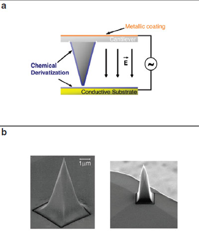
Figure 1 a)- Scheme of an AFM probe used in
this study with the associated electric field. b) SEM
images of a modified cantilever.
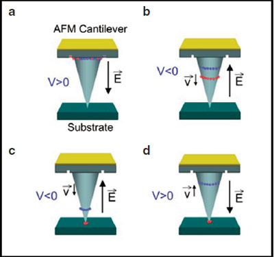
Figure 2- Depending on the voltage pulse and
polarity, molecules (red) may be released from the tip
and deposited on the substrate.
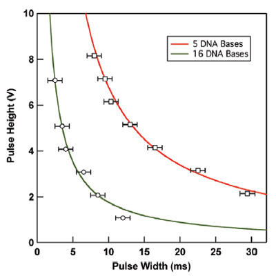
Figure 3- The different mobilities of 5- and 16-
base DNA fragments enable their separation using
this AFM-based electrophoretic technique.
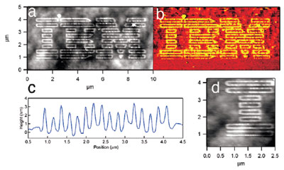
Figure 4- Topographic (a) and lateral force (b)
images showing controlled surface patterning with
5-base-long DNA fragments. Line scans (c and
d) show a mean height of 2.4 nm and line width of
between 59 and 79 nm.
The technique works because of
the thin film of water found on
the substrate and on the probe
itself (Figures 1–4 display the
ultrafast molecule sorting story). By
applying a field between a conducting
cantilever and probe and the
conducting substrate, it is possible to
exploit the electrophoretic mobilities
of molecules. Thus, by varying
field strength and polarity, it is possible
to precisely control deposition
and removal of the molecules
from the surface. When this is combined
with the positioning capabilities
of a modern AFM system, it is
possible to envision a method that
writes features five times smaller than
today’s e-beam lithography and 10
times smaller than photolithography.
It is the control of the thin film of
water through control of the humidity
of the experiment that makes this
method work.
Understanding the chemistry of
the process is also extremely important.
Close control of the probe
and surface chemistries is required
to ensure the molecules are immobilized to prevent diffusion. In
the experiments used to illustrate
this inkjet concept of writing, Dr.
Wickramasinghe’s team investigated
single-stranded DNA fragments.
Deposition was confirmed
using lateral force microscopy
(LFM) because it is particularly
sensitive to frictional change, thus
readily “seeing” the sticky molecules
on the smooth substrate.
The electrophoretic AFM method was
compared to traditional capillary electrophoresis.
The transfer times using
AFM were dramatically reduced: A
15-base-long strand of DNA could
be transferred in 5 msec compared to
170 sec in a conventional 8.5-cm-long
microfluidic channel.
The potential impact of this work
ranks alongside some of Dr. Wickramasinghe’s
other achievements.
The method has enabled the acceleration
of molecular separation,
and transfer has been speeded up
by several orders of magnitude.
Dr. Wickramasinghe believes this
wi l l have an impa c t on futur e
research in biology and medicine.
For example, DNA sequencing will
be speeded up through reduction
in sample size. The method is very
scaleable using either multiple-tip
arrays or multiple reservoirs with
different molecules.
It is work like this that makes
exploring the field of SPM so exciting.
With nanotechnology already
being part of today’s world, it is the
work of scientists like Dr. Wickramasinghe
that emphasizes the benefits
of working on the nanoscale
to enhance the quality of life today
and for generations to come. So
what will the next 25 years bring?
The only restriction is the power of
our imagination.