In recent years, carbon nanomaterials have created their own niche in materials science due to their exceptional electronic, thermal, mechanical, optical, and magnetic properties, creating potential applications in a wide range of fields, including electronics, energy conversion and storage, sensing, and drug delivery. Raman spectroscopy is an integral part of carbon nanomaterial research because it plays a vital role in the characterization of these materials. In sp2-bonded carbon species, this highly sensitive technique can be used to evaluate the 1) number of layers, 2) type and relative quantity of defects, 3) mechanical strain, and 4) functionalization and doping in addition to several other parameters that are specific to each carbon nanomaterial.
 Figure 1 – Raman spectrum of a graphene film and a carbon nanotube with the 2D, G, and D bands labeled. The inset shows the radial breathing mode of a carbon nanotube as well as the splitting of the G band into the G- and G+ peaks.
Graphene is a two-dimensional carbon allotrope that consists of a one-atom-thick, hexagonal array of sp2-bonded carbon atoms. The Raman spectrum of graphene has three prominent peaks, known as the 2D, G, and D bands, as shown in Figure 1. The 2D and G bands are present in all graphene samples, whereas the D band is only activated if defects are present. The intensity ratio of the D and G Raman peaks provides a method to qualitatively compare the defect density between graphene samples, in which a larger D to G ratio indicates a higher defect density. In addition, the width and shape of the 2D peak are used to characterize the number of graphene layers.
For monolayer graphene, the full width at half maximum is around 30 1/cm, and the peak can be fit with a single Lorentzian curve.1,2 As the number of graphene layers increases, the full width at half maximum increases and the peak splits into more components due to band splitting in the graphene electronic structure. Furthermore, the position of the 2D and G bands can be used to quantify the strain and doping in graphene films. Depending on the relative shift of the 2D and G peaks and the direction of the shift of the 2D band, the effects of strain and doping can be determined.
Carbon nanotubes are a one-dimensional carbon allotrope and can be conceptualized as a graphene sheet that has been wrapped to form a cylinder. The Raman spectrum of a carbon nanotube has similar features to that of graphene and additional peaks known as radial breathing modes (Figure 1 inset). The position of the radial breathing mode allows the nanotube diameter to be determined. The one-dimensional character of nanotubes gives rise to an additional G peak called the G- peak (Figure 1 inset), which can be used to distinguish metallic and semiconducting nanotubes.
A more comprehensive review of the theory behind Raman imaging of carbon nanotubes can be found in an article by Dresselhaus et al.3 Here, we present examples from our research of how Raman imaging can be used to 1) minimize the defect density in graphene films grown via chemical vapor deposition, 2) study diffusion of oxygen through defects in graphene, and 3) characterize the electronic nature of carbon nanotubes. Raman imaging is a technique in which Raman spectra are collected at multiple predetermined locations on the sample to spatially map the material properties.
Optimization of graphene chemical vapor deposition conditions
Raman imaging provides spatially resolved chemical information about graphene crystals, including the number of graphene layers and the defect density. In this work, Raman imaging is used to provide the feedback required to optimize the graphene synthesis conditions via chemical vapor deposition to achieve high-quality graphene films with reduced defect density and, thus, superior properties.
Chemical vapor deposition is an inexpensive, scalable method to produce large-area graphene films.4 During deposition, carbon precursors are catalytically converted into sp2 carbon on a metal substrate, such as copper, to form graphene. Unfortunately, defects are incorporated into the graphene lattice, which degrades the excellent properties of graphene.
Consequently, an incredible amount of effort has been spent to decrease the number of defects introduced during growth. Simultaneously, researchers have been attempting to decrease the synthesis temperature to make the process more suitable for industrial scale production. However, previous attempts to create high-quality graphene at low temperatures have typically failed.
Here, we systematically varied the growth temperature, precursor flux, and catalyst surface orientation and stopped the growths before a continuous monolayer of graphene formed. In these partial growth samples, Raman imaging provides information about the graphene nucleation density, coverage, and island morphology in addition to the number of graphene layers and defect density. The graphene crystals on copper substrates were characterized with Raman imaging using a Thermo Scientific™ DXR™xi Raman imaging microscope (Thermo Fisher Scientific, Madison, WI) with excitation wavelength of 455 nm to reduce fluorescence from the copper substrate. The reduced fluorescence and fast scan rate allow us to study the graphene crystals directly on copper substrates, rather than transferring them to silicon dioxide or a similar substrate in which the Raman signal is enhanced. The transfer process introduces unwanted defects and contamination to the graphene films and, therefore, makes the Raman spectra more difficult to analyze. Therefore, this Raman system enables us to study the pristine graphene crystals on the catalyst on which they were grown.
 Figure 2 – Raman map of the 2D band (2728 1/cm) of graphene crystals grown on copper. The green and blue areas are graphene and copper, respectively. This map provides critical information about the number of graphene layers, defect density, nucleation density, coverage, and island morphology to allow us to optimize the synthesis conditions.
Figure 2 shows a Raman map of the 2D band (2728 1/cm) of graphene crystals grown on the (110) face of copper. The D band intensity is negligible, revealing the low defect density in these graphene films (Figure 1). The narrow full width at half maximum and Lorentzian shape confirm that the graphene crystals consist entirely of a single layer. Raman imaging also provides spatial information about the graphene samples. Using Raman imaging, we determined that the graphene nucleation density and coverage are 105 nuclei/cm2 and 75%, respectively. The graphene crystals are rectangular, which reflects the symmetry of the underlying copper (110) lattice.5
Raman imaging of graphene crystals grown with different synthesis conditions allowed us to gain novel insight into the critical chemical vapor deposition parameters that affect the graphene crystal growth. Furthermore, we used this knowledge to optimize the growth conditions to yield high-quality, monolayer graphene at temperatures that are around 250 °C lower than what is typically used for graphene synthesis using the same carbon precursor. The understanding gained from this growth optimization using Raman imaging feedback will improve the scalable crystal growth engineering of graphene, as well as other two-dimensional materials. Ultimately, we hope that our work will help enable the first generation of graphene-based technologies.
Diffusion of oxygen through defects in graphene
In addition to providing information about the spatial distribution of defects in graphene films, Raman imaging also has the ability to map the location of chemical compounds due to their unique Raman signatures. For example, when a piece of copper is annealed in air at 200 °C, oxygen and water vapor readily react with the surface of copper to form copper oxide (Cu2O), among other species, in a few minutes. The existence of Cu2O on the surface of copper is easily verified by the presence of a Raman peak at 647 1/cm. However, when a layer of graphene is placed on the surface of copper and the sample is subjected to the same treatment, the oxidation of the copper surface is greatly reduced, suggesting that the graphene layer is able to block most of the gaseous oxygen and water vapor from reaching the surface of the copper and, thus, acts as a diffusion barrier.
 Figure 3 – Scanning electron micrograph showing the surface of a) as manufactured bare copper foil, b) as-manufactured graphene on copper foil (grown via chemical vapor deposition), c) bare copper foil annealed in air, d) graphene on copper annealed in air (scale bars = 2 μm), and e) Raman line scan across a grain-like feature in an annealed graphene film on copper.
Figure 3a–d shows scanning electron micrographs of bare copper and graphene on copper before and after annealing in air. The surface of the copper is completely oxidized without graphene (Figure 3c). However, in the presence of graphene, the oxidation of the copper surface is greatly reduced and is restricted to grain-like features (Figure 3d).
Graphene has the potential to be an ideal diffusion barrier because it is impervious to species as small as atomic helium due to its short (1.42 Å) carbon–carbon bond distance. This unique property inherently makes graphene an attractive choice for applications like corrosion inhibition of reactive/refined metals, lifetime enhancement of organic photovoltaic devices, and ultrahigh sensitive gas detection.6 However, in reality, the graphene lattice is riddled with defects and grain boundaries, which provide spurious transport pathways through which gases can percolate and, hence, limit barrier performance.
Even though the graphene sheet protects the underlying copper from oxidation, the defects in the graphene layer provide diffusion pathways through which oxygen and water can percolate and oxidize the surface.
In order to better understand and visualize these transport pathways through graphene, it is essential to spatially map transport through the graphene membranes. Raman imaging with the DXRxi Raman imaging microscope was used to identify defective regions in the graphene layer via spatially mapping the D band (1345 1/cm) to G band (1585 1/cm) intensity ratio (as mentioned in the previous section) and also Cu2O (647 1/cm), hence enabling us to correlate the oxidation of the copper surface to the defects and grain boundaries in the graphene film.
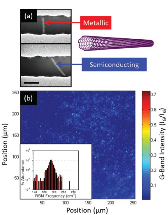 Figure 4 – a) Scanning electron micrograph (scale bar = 100 nm) of a carbon nanotube array field-effect transistor with metallic and semiconducting nanotubes spanning the channel of different devices. b) Raman map of a spin-cast carbon nanotube film with approximately 64,000 individual nanotubes. Inset shows radial breathing mode histogram of 9000 nanotubes.
Figure 3e shows a Raman line scan across an edge of a grain-like feature of an annealed graphene on copper sample in which the color depicts the intensity of the Raman signal normalized to the G peak of graphene. An increase in the D peak (graphene defect peak at 1345 1/cm) intensity is observed in the same region where there is an increase in the Cu2O intensity (647 1/cm), illustrating that the underlying copper locally oxidizes underneath defects and grain boundaries in the overlying graphene and thus confirming that the primary mode of oxygen transport through the graphene is through these features.7 In addition, Raman imaging helps us to relatively quantify the amount of oxidized copper, enabling us to evaluate the barrier performance. Specifically, our studies show that the spatially averaged intensity of the Cu2O Raman peak is reduced by a factor of 11 when covered by a single layer of graphene after 120 minutes of annealing. Raman imaging not only helps us by providing crucial insight about transport through graphene membranes, but in the future this technique can also serve as a foundation for tailoring and characterizing high-quality diffusion barriers using graphene atomic membranes.
Electronic nature of carbon nanotubes
Raman imaging is a valuable tool for applications that require detailed spatial resolution and large-scale quantification of chemical and structural features. By taking Raman maps with a step size of 200 nm, we are able to individually characterize carbon nanotubes in films while mapping their cumulative spatial distributions. By analyzing all of the spectra for individual nanotubes, we can understand a wealth of information, such as the electronic type purity, diameter distribution, and defect density of over 10,000 carbon nanotubes in a single measurement.
We have coupled the electronic measurement of nanotubes in field-effect transistor devices with Raman imaging as a powerful tool to accurately quantify the metallic to semiconducting nanotube ratio of thin carbon nanotube films. The G band in carbon nanotubes is composed of two peaks: the G+, which derives from phonon dispersions along the nanotube axis; and the G-, which is influenced by the electronic type and diameter of the nanotube.3 In metallic nanotubes, the G- peak broadens and the Raman intensity increases due to the overlap of energy bands and lack of band gap. The difference in the metallic and semiconducting Raman spectra is shown in the inset of Figure 1, where the electronic properties of carbon nanotubes contained within an array of field-effect transistors (Figure 4a) are confirmed by analysis of the Raman G- peak. We used this experimental technique to quantify the purity of 10,000 nanotubes demonstrating a semiconducting purity of 99.8%.
We have developed methods to sort nanotubes by diameter, chirality, and electronic type for electronic applications such as solar cells and transistors. It is desirable to sort heterogeneous mixtures of nanotubes so that the nanotubes all have a similar band gap for consistent electronic performance. Raman imaging can be used as a tool to quantify the extent of sorting, and the radial breathing modes can be extracted in order to obtain a distribution of the nanotube diameters contained in a sample.
A large-area Raman map of a nanotube film with an approximate density of 1 nanotube/μm2 is shown in Figure 4b. Further analysis of the spectra at each pixel is achieved by extracting the radial breathing mode of 9000 nanotubes shown in the histogram in the inset of Figure 4b. We sorted a range of nanotube diameters from 1 to 1.5 nm, which is reflected in the range of radial breathing modes.
Conclusion
Recent advancements in Raman imaging have directly impacted the scale to which carbon nanomaterials can be characterized, enabling the characterization of graphene films and carbon nanotubes over large sample areas in a short time period. Our research provides an example of how Raman spectroscopy will continue to facilitate the advancement of cutting-edge nanotechnology research in the future.
References
- Malard, L.M.; Pimenta, M.A. et al. Raman spectroscopy in graphene. Physics Reports—Review Section of Physics Letters 2009, 473, 51–87.
- Ferrari, A.C. Raman spectroscopy of graphene and graphite: disorder, electron-phonon coupling, doping and nonadiabatic effects. Solid State Communications 2007, 143, 47–57.
- Dresselhaus, M.S.; Dresselhaus, G. et al. Raman spectroscopy of carbon nanotubes. Physics Reports—Review Section of Physics Letters 2005, 409, 47–99.
- Li, X.S.; Cai, W.W. et al. Large-area synthesis of high-quality and uniform graphene films on copper foils. Science 2009, 324, 1312–14.
- Jacobberger, R.M.; Arnold, M.S. Graphene growth dynamics on epitaxial copper thin films. Chemistry of Materials 2013, 25, 871–7.
- Singha Roy, S.; Bindl, D.J. et al. Templating highly crystalline organic semiconductors using atomic membranes of graphene at the anode/ organic interface. J. Phys. Chem. Letters 2012, 3, 873–8.
- Singha Roy, S.; Arnold, M.S. Improving graphene diffusion barriers via stacking multiple layers and grain size engineering. Adv. Functional Materials 2013, 23, 3638–44.
Gerald Brady, Robert Jacobberger, Susmit Singha Roy, and Michael Arnold are with the Department of Materials Science and Engineering, University of Wisconsin—Madison, 1509 University Ave., Madison, WI 53711, U.S.A.; e-mail: [email protected] . Gerald Brady, Robert Jacobberger, and Susmit Singha Roy contributed equally to this work. Mark Wall is with Thermo Fisher Scientific, Madison, WI, U.S.A. Section I was supported by the DOE Office of Science Early Career Research Program (grant no. DESC0006414) through the Office of Basic Energy Sciences. Section II was supported by the National Science Foundation Grant #CBET-1033346. Section III was supported by National Science Foundation Grant #CMMI-1129802. R.M.J. acknowledges support from the Department of Defense (DOD) through the National Defense Science & Engineering Graduate Fellowship (NDSEG) Program.