Microscopy is often overlooked at Pittcon®, yet of the 12,000+ scientists who attend, approximately 30% use microscopy in some form (according to ongoing research from The Microscopy & Imaging Place, Inc., www.the-mip.com). As clearly demonstrated by the technologies covered in this article, microscopy has become part of the routine analytical scheme. It brings eyes to chemistry, allowing researchers and technologists to see particle size, shape, and distribution; measure spectra on the micro- and nanoscale; and observe processes and properties like never before.
Particle analysis and electron microscopy will both be hot topics at Pittcon 2014, with a number of companies having working systems on the show floor. MicroRaman will also be strong, with interesting new hybrids such as Raman/AFM. And there is something new under the sun in that good old workhorse, light microscopy: Microscopes that are especially comfortable, new camera/communication hubs, and new exhibitors in calibration.
Here’s a quick overview of over two dozen microscopy and related imaging technologies that will be on display on the show floor. Within each technology sector, companies are presented alphabetically. And don’t miss the special educational opportunities listed at the end of the article.
Fluid Imaging Technologies debuts new AutoFocus
 Figure 1 – Fluid Imaging Technologies introduces FlowCAM with AutoFocus.
The FlowCAM® imaging particle analyzer from Fluid Imaging Technologies (www.fluidimaging.com) is now available with an AutoFocus feature (Figure 1). This upgrade makes the system even easier to use, and provides a consistent and repeatable fine focus with minimal user interaction.
The AutoFocus Assistant provides on-screen, step-by-step instructions to walk you through the process. Using VisualSpreadsheet® to calculate the ideal focal position, the new AutoFocus assures consistent, repeatable focus every time.
Booth #1656
HORIBA announces the new ParticleFinder
HORIBA’s (www.horiba.com/us/en) new ParticleFinder software module (Figure 2) automates particle location and chemical characterization. In combination with HORIBA Raman microscopes (see Spectroscopy, below), ParticleFinder brings a new level of automation and ease of use for particle analysts. It is ideally suited for locating and identifying particulate matter where automated molecular analysis is key, especially for pharmaceutical materials, trace forensic evidence, geological rock/mineral particles, and airborne contaminants trapped on filters.
Booth #2102, 2202
 Figure 2 – HORIBA adds ParticleFinder to Raman.
Malvern features Morphologi G3 and Nanosight particle tracking
The Morphologi G3 automated image analysis system from Malvern (www.malvern.com) is an advanced particle characterization tool for the measurement of particle size and particle shape distributions from 0.5 microns to several millimeters. It offers the flexibility of operation and validation required to support both R&D and automated QC applications. The Morphologi G3-ID adds Raman spectroscopy, delivering component specific size and shape data required to fully understand how formulation and manufacturing methods affect downstream processability and end-product bioavailability.
Also new in the Malvern booth is its recent acquisition: nanoparticle tracking from NanoSight (www.nanosight.com). NanoSight CEO Jeremy Warren reports, “We have always seen Malvern as our natural home. The fit of Nanoparticle Tracking Analysis (NTA) into the Malvern characterization range is crystal clear, plus NTA adds unique nanoparticle counting and concentration measurement. NanoSight will continue as a brand within Malvern, whilst taking advantage of the reach and depth of Malvern’s global channels.”
Booth #1648
Microtrac launches new suite, including 3D Image Analyzer
Microtrac (www.microtrac.com) is a pioneer in laser diffraction and DLS (dynamic light scattering) instrumentation. New additions in the Microtrac booth at Pittcon include the DLS particle size analyzer with cuvette sample cell, 3D Image Analyzer with online capability, particle charge titration analyzer, and a full suite of surface area analyzers. These analyzers are ideal for QC and R&D professionals. Bring your samples for a complimentary sample analysis.
Booth #3213
Phenom-World unveils ParticleMetric software
Phenom-World (www.phenom-world.com) is launching the new ParticleMetric software for fully automated visualization and analysis of particles and powders. ParticleMetric is based on SEM (scanning electron microscopy) imaging, allowing the user to identify phenomena such as broken particles, agglomerates, and foreign particles that can lead to new discoveries and innovations in powder design, development, and quality control. The fully automated measurements show different particle features such as particle shape, surface area, circularity, circumscribed circle diameter, and convexity can easily be correlated and reported.
Booth #550
Carl Zeiss features fully correlated LM, EM, and X-ray microscopies
Experience the ultimate in materials characterization by imaging exactly the same sample area with X-ray, light, and electron microscopes. This year at Pittcon, Carl Zeiss (www.microscopy.zeiss.com ) brings together results from the Axio Imager and Axio Zoom Light Microscopes (LM), the brand new EVO Scanning Electron Microscope (SEM), and Xradia X-ray microscopes (XRM) for remarkably improved throughput and analyses (Figure 3).
 Figure 3 – Carl Zeiss correlates workflow between light, electron, and X-ray microscopy.
Zeiss acquired Xradia X-ray microscopy in 2013, introducing two new nondestructive 3-D imaging systems for synchrotron-quality lab-based research. Xradia 520 Versa offers submicron imaging with unique dual-energy-based compositional contrast capability. Xradia 810 Ultra provides <50 nm spatial resolution up to 10× faster for a wide variety of materials.
Also this year at Pittcon, Zeiss introduces its fourth-generation EVO Series SEM, achieving superior low voltage (1 kV) resolution (twice that of the previous generation), and setting an unmatched standard for tungsten and LaB6 source SEMs. SmartSEM7 enables rapid throughput featuring EasyVP simple-to-use variable pressure electron optics, intelligent SmartBrowse imaging, automatic aperture alignment, and Drift Corrected Frame Averaging.
Booth #4639
EDAX launches new Silicon Drift Detectors
EDAX, Inc. (www.edax.com), well-known for its X-ray microanalysis and electron diffraction instrumentation, introduces a new series of detectors for the transmission electron microscope into its highly successful Octane Silicon Drift Detector (SDD) family (Figure 4). Based on the state-of-the-art design of the company’s Octane SEM series, the Octane TEM portfolio offers three models to meet the needs of all TEM applications. The Octane TEM SDD family is paired with EDAX’s TEAM™ EDS software, allowing users to optimize their analysis time and get the best data possible from their samples.
Booth #3931, 4031
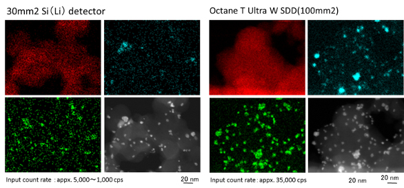 Figure 4 – Comparison of a 30-mm2 Si(Li) detector to EDAX’s new Octane T Ultra W SDD (100 mm2).
FEI suite of solutions includes SEM, TEM, dual beam, and VSG software
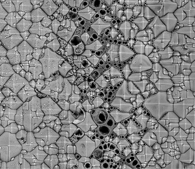 Figure 5 – SEM image of a solar cell. Image courtesy of FEI.
FEI (www.fei.com) delivers solutions for characterization of a broad range of materials including powders, polymers, particles, ceramics, catalysts, solar, and fuel cell materials (Figure 5). FEI’s environmental microscope solutions provide in situ, dynamic observation of material performance under environmental influences or near-real operating conditions to yield critical information about performance and lifetimes of functional materials. FEI’s SEM, TEM (transmission electron microscope), and DualBeam FIB/SEM instruments excel in producing the highest-quality images and analytical results from beam-sensitive or soft materials, as well as for metals and alloys.
VSG, acquired last year by FEI, will also exhibit. VSG Avizo software processes and segments multimodality data from tomography, microscopy, MRI, etc. In addition to advanced measurement and quantification and porous and multiphase media analysis, Avizo offers 3-D model reconstruction and 3-D image-based meshing for CFD (computational fluid dynamics) and FEA (finite element analysis). For researchers and engineers involved in computation chemistry, there are also functions for materials properties simulation direct from 3-D images and simulation pre- and postprocessing tools.
Booth #3709
JEOL USA announces the iT300LV SEM
JEOL (www.jeol.com) announces the iT300LV SEM, featuring a sleek tablet interface design and intuitive operation for imaging a wide range of samples. The microscope’s smart analytical port geometry accommodates 10 or more attachments, including dual EDS (energy-dispersive X-ray spectrometer) systems at a working distance of 10 mm for high-throughput microanalysis. The unique in-chamber five-axis motorized stage ensures fast asynchronous movement and accurate sample positioning even for large, nonuniform samples. The iT300LV SEM features accelerating voltages from 300 to 30 kV, pressures from 10 to 650 Pa, and a magnification range from 5 to 300,000×.
Booth #3241
TESCAN presents VEGA LMU
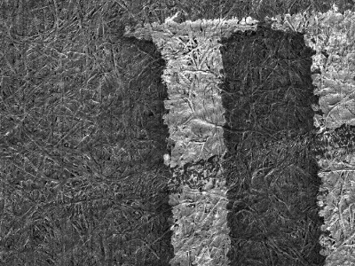 Figure 6 – SEM image of crossed lines, toner print over signature. Image courtesy of TESCAN USA.
TESCAN USA (www.tescan.com) will present the VEGA LMU, which is applicable to a wide range of SEM applications and needs in today’s research and industry (Figure 6). The VEGA offers a unique four-lens Wide Field Optics™ design offering a variety of working and displaying modes. The proprietary Intermediate Lens (IML) functions as an “aperture changer” to adjust the effective final aperture electromagnetically. Unique live stereoscopic imaging using advanced 3D Beam Technology opens up the micro and nanoworld for an amazing 3-D experience and 3-D navigation. The VEGA offers several optional modules or dedicated applications optimized for automatic sample examination procedures, such as morphology and particle analysis and 3-D surface reconstruction, etc.
Booth #563
KEYENCE showcases imaging and metrology for industrial applications
 Figure 7 – Digital image of needle. Image courtesy of KEYENCE.
KEYENCE (www.keyence.com), widely known for its digital microscopes, will be showcasing its latest imaging and metrology equipment for industrial applications. These systems provide users with the ability to perform 360º inspection on objects with magnifications from 0.1× to 5000×, allowing for calibrated surface measurements from nanometers to millimeters (Figure 7). Unlike most systems that can be complicated to operate, KEYENCE microscopes are extremely easy to use so that anyone can capture high-quality 2-D/3-D images.
Booth #2318
Olympus IMS takes measuring and opto-digital imaging to the next level
 Figure 8 – 3D Measuring & Opto-digital Technology from Olympus: LEXT confocal and DSX Opto-digital microscope.
By combining the observation strength of light microscopy with the convenience of advanced digital technology, Olympus (www.olympus-ims.com) is delivering a new level of operator simplicity with no sacrifice in image quality, speed, or accuracy. Designed for quality assurance and control labs, the Olympus DSX Series of opto-digital microscopes captures clear images, acquires reliable measurements, and delivers reproducible results, all with the tap of a touchscreen (Figure 8). The Olympus LEXT OLS4100 opto-digital laser confocal microscope system meets the demand for increased measurement precision through nanometer-level imaging, accurate 3-D measurement, and outstanding surface roughness analysis.
Booth #4539
Vision Engineering’s new Ergo80 stereo provides comfort and quality imaging
If you are looking for comfort in microscopy viewing, visit Vision Engineering (www.visioneng.com). Its Ergo80 stereomicroscope employs a revolutionary patented eyepiece design that does not require users to precisely align their eyes with the eyepieces. In fact, the user can sit back from the microscope (up to 1.5”) and still view the image, meaning that uncomfortable and difficult-to-use eyepieces are a thing of the past. It is worth a visit to this booth just to feel the difference between conventional oculars and these ultrahigh-point systems.
The high-quality designed CMO stereomicroscope offers 8× to 64× standard magnification range (128× max.), with patented ergonomic eyepieces to reduce fatigue, and an ergonomic working position that offers freedom of head movement. The light source provides long life (2000 hr) and true color illumination. A modular system readily connects optional extras to configure more detailed setups.
Booth #4759
Bruker sets new standards with PeakForce Tapping® AFM
Proprietary PeakForce Tapping from Bruker (www.bruker.com) opens the door to research possibilities that were once considered beyond the reach of atomic force microscopy (AFM) (Figure 9). PeakForce Tapping has set a new standard and is now the principal AFM mode for research, with the fastest growing publication record. Operating at the lowest forces, it uniquely provides a combination of the best quantitative and highest-resolution AFM data available for mechanical, electrical, and topographic-related applications.
Booth #4135
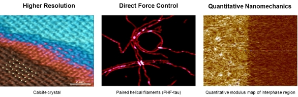 Figure 9 – Results from Bruker’s new PeakForce Tapping. Left: Single-point atomic resolution. Center: low imaging forces. Right: real-time quantitative modulus mapping.
Spectroscopy
BaySpec features high-resolution, multilaser micro-Raman
BaySpec (www.bayspec.com) will feature its high-resolution multilaser Raman microscope, Nomadic™. Continuously evolving from last year, the Nomadic multiexcitation confocal Raman microscope now includes a high-resolution (2 cm–1), AFM-ready, large frame for wafers and retrofitting options. The new system has inherited all the power of its predecessor, including multiple laser excitations from UV to NIR with pushbutton switching, fully automated operation, and unmatched sensitivity and speed implemented using BaySpec’s highly efficient proprietary VPG® technology. The 2014 Nomadic is the ultimate Raman microscope for the most challenging analysis in your laboratory.
Booth #2119
B&WTek presents handheld system
B&WTek (www.bwtek.com) is known for handheld Raman and now has intriguing accessories to convert simple microscopes to Raman. New on the handheld side: NanoRam FP, with a flexible fiber optic probe that is perfect for hard-to-reach places as well as disposable sleeves for the B&WTek immersion shaft accessory (available with both of its NanoRam products) to reduce cross-contamination between measurements.
Booth #4214
HORIBA expands Raman and AFM/Raman
HORIBA’s XploRA-nano is a powerful instrument that combines Raman spectroscopy and scanning probe microscopy (SPM) into a single integrated platform to analyze the same sample with both techniques simultaneously (Figure 10). Raman, being a light-based technique, is limited in spatial resolution by diffraction, but with the latest advance in tip-enhanced Raman and probes solution from HORIBA, nano-Raman down to ~10-nm resolution is now within the reach of most scientists. It is the new standard when it comes to label-free chemical imaging at the nanoscale.
 Figure 10 – Two new microRaman systems from HORIBA: a) XploRA-nano, and b) XploRA PLUS.
The XploRA PLUS from HORIBA Scientific incorporates unique and powerful functions in a high-performance system. Fully confocal, it does not compromise image quality, spatial, or depth resolution. SWIFT™ Fast Raman imaging offers the best, most detailed Raman images, typically 10× faster than the competition! Enhanced range of options such as multiple laser wavelengths, EMCCD (electron multiplying charge coupled device) detection, Raman polarization, and AFM coupling means that, for multisample and multiuser environments in research and analytical labs, XploRA Plus is the uncompromising choice.
LabSpec 6, a complete Raman software application, guides researchers through system setup, Raman spectrum data/map acquisition, measurement and data processing, and report generation.
Booth #2122, 2202
Building upon the high-performance capabilities of the NRS-5000/7000 series Raman instruments, JASCO (www.jascoinc.com) has released the new compact and easy-to-use NRS-4100 Series Laser Raman Spectrometer. The NRS-4100 has many of the great features and performance of its larger siblings, with a whole host of new technological innovations.
Measuring just 24 cubic inches, this system is truly compact and lightweight. Up to three excitation lasers can be selected with a range of wavelengths from the visible to the NIR. The NRS-4100 incorporates a 200-mm spectrograph with the ability to include up to four gratings on a selectable turret to provide resolution down to 0.7 cm–1/pixel.
Automatic optical-path alignment is included as standard and can be executed from a single mouse-click in the Spectra Manager II software. Find out more at www.jascoinc.com/nrs-4100.
Booth #3639
Renishaw highlights inVia research Raman microscope
Renishaw (www.renishaw.com/invia) will feature the inVia research Raman microscope. Fully configurable, this flexible research stand includes excitations from UV through NIR, 2-D/3-D fast imaging, and near-excitation analysis, with accessories and microscope configurations to suit all application areas from nanomaterials to biology. inVia provides a nondestructive means of obtaining chemical/molecular information, with submicrometer spatial resolution. Combine inVia with other techniques to perform co-localized sample analysis, including SPM/AFM/TERS (tip-enhanced Raman spectroscopy), SEM, and CLSM (confocal laser scanning microscopy).
Booth #1816
Thermo Scientific launches DXRxi Raman Imaging Microscope
Materials scientists, engineers, and academic researchers can now accelerate their research and increase their productivity using the Thermo Scientific DXRxi from Thermo Fisher Scientific (www.thermoscientific.com), a powerful new Raman imaging microscope that doesn’t require Raman expertise to master. The instrument, which rapidly delivers research-grade imagery of a material’s molecular structure and chemical composition, has applications in many industries, including pharmaceutical formulation, semiconductor manufacturing, life sciences, and geology.
With instant visual feedback and intuitive image-driven controls, the Thermo Scientific DXRxi Raman imaging microscope offers unrivaled simplicity and approachability that enables scientists of all abilities and disciplines to access the benefits of Raman imaging without a learning curve. Users will advance research faster, publish more, and solve problems more confidently than previously possible with Raman imaging.
Accessories
89 North highlights first direct-mount metal halide light source
The PhotoFluor 75 from 89 North (www.89North.com) is the first metal-halide light source that mounts directly on your microscope—no more liquid light guides. With its small, space-saving footprint, silent operation, and efficient DC ballast, the powerful LM-75 provides unmatched stability. 89 North provides intelligent solutions for your microscopy illumination needs. The company also distributes state-of-the-art, low-maintenance imaging products from Cairn Research (www.cairn-research.co.uk), including easy-to-use modular image-splitters, filter wheels, and a multiline laser launch system.
Booth #2152
APPLIED IMAGE brings new calibration to light microscopy
 Figure 11 – Today’s more complex measurement needs require more sophisticated NIST and ISO certified standards, such as those from APPLIED IMAGE.
Calibration in the 21st century is no longer a simple subjective determination. In the past, all that was required was a linear scale and a reticle, but this approach is no longer adequate for today’s complex electronic imaging systems. Today’s systems require NIST- or ISO-certified standards for additional calibration of the limiting resolution, contrast capabilities and colors for most instruments. APPLIED IMAGE (www.aig-imaging.com) provides a wide range of standards to meet these needs (Figure 11). In addition, APPLIED can design and manufacture a custom calibration standard to your specific requirements.
Booth #2565
Motic advances digital wireless platform
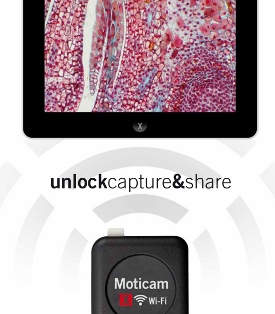 Figure 12 – Motic’s digital wireless platform for industrial, educational, and clinical labs.
With the advancement of the digital age in our personal lives, Motic (www.motic.com) introduces a new Moticam X camera series that frees the viewer from traditional wired connections (Figure 12). Using standard “free” downloadable viewers for any Android or iOS platform, real-time images can be shared from any microscope simultaneously for educational to consultative dialogues to up to six viewers—more if a MoticHUB is used.
Moticam X is the standard Moticam that can be connected to any microscope. It comes with Motic Images Plus 2.0 for running on a Laptop with WiFi. Users can also download and use iOS and Android Apps FOC to view streaming images, capture, and measure.
MoticHUB is a software-based application that can connect any Moticam or digital microscope running Motic software to iOS and Android tablets through WiFi.
Booth #4364
USHIO announces new fiber-optic LED light sources
The Midori™ ULB 35i fiber-optic LED light source from USHIO America (www.ushio.com) is a compact and lightweight fiber-optic illuminator, with high output efficacy, ideal for microscopy or other fiber-optic applications where space is at a premium. This mercury-free, long-life ULB35i LED light source has instant-on and electronic intensity dimming capabilities. Midori’s spectral output below 430 nm and above 700 nm is minimal.
The Midori unit is equipped with an ACMI fiber receptacle, and separate Storz or Olympus style adaptors to accommodate most common fiber cable types.
Booth#1854
Educational opportunities
Anasys
Pittcon nanoIR scientific talks on biofuels, composites, fuel cells
Expanding Applications for AFM-Based Infrared Nanospectroscopy
Sunday, March 2, 1:30 PM (100-1), Session 100, Room S404d
Speaker: Craig Prater, Anasys Instruments
Characterization of Materials Using AFM-Based Nanomechanical, Nanothermal, and Nanoscale
Infrared Spectroscopy and Imaging
Sunday, March 2, 2:30 PM (100-4), Session 100, Room S404d
Speaker: Curtis Marcott, Light Light Solutions
Nanoscale Dynamic Mechanical Spectroscopy of Polymer Blends and Composites
Sunday, March 2, 1:30 PM (230-1), Session 230, Room S504bc
Speaker: Eoghan Dillon, Anasys Instruments
Nanoscale Infrared Spectroscopy of Fiber Composite Materials
Wednesday, March 5, 9:10 AM (1630-3), Session 1630, Room S504d
Speaker: Michael Lo, Anasys Instruments
For more information, visit http://www.anasysinstruments.com/pittcon_2014.
B&WTek
SAS Women in Spectroscopy Session
Thursday, March 6, 8:30 AM, Room S405b
Katherine Bakeev from B&WTek will be one of numerous speakers for the Women in Spectroscopy Session. Career options, academic experiences, and much more will be discussed in this half-day symposium. Admittance is free of charge, but be sure to get to Room S405b early if you want a seat, as this session is expected to fill up fast!
For more information, visit https://www.s-a-s.org/for-members/women-in-spectroscopy.
Hitachi will present daily Learning Labs
Thermal Analysis w/Real View Technology
Monday, March 3
SEM Fundamentals
Tuesday, March 4
X-Ray Fluorescence and Forensics
Wednesday, March 5
For registration and details, visit Booth #3624.
Horiba
Japan Symposium: “The State-of-the-Art Technologies that support Safety and Security in Future”
Tuesday, March 4, two sessions: 8:30–11:30 AM and 1:30–4:30 PM, Room S505b
HORIBA Scientific’s Sergey Mamedov will be speaking at 2:45 on “Microspectroscopy for Trace Analysis in Forensic Science.”
For more information, visit http://www.horiba.com.
Malvern Short Courses
Sampling for Particle Size Analysis
Saturday, March 1, 8:30 AM
Instructor: Dr. Alan Rawle
Learn the basics and importance of sampling for particle size analysis. Find out how to better determine the minimum mass needed for any required precision and how to calculate the best fundamental sampling error.
For registration and details, visit: http://ca.pittcon.org/Technical+Program/tpabstra14.nsf/SCoursesByCat/561FC4A974FC0CF885257B83006927E3?opendocument.
Particle Characterization of Nanomaterials
Wednesday, March 5, 8:30 AM
Instructor: Dr. Ana Morfesis
Understand particle size, molecular weight, and formulation stability as it relates to your application using DLS and ELS techniques. Different application and data interpretation examples will be presented.
For registration and details, visit: http://ca.pittcon.org/Technical+Program/tpabstra14.nsf/SCoursesByCat/6218A094F7B30C6E85257B87000FEC20?opendocument.
Fundamentals of Particle Size Analysis with an Emphasis on Light Scattering Techniques
Thursday, March 6, 8:30 AM
Instructors: Drs. Alan Rawle and Ulf Nobbmann
In this full-day course, learn all the basics about particle sizing—technology, terminology, international standards, and math. Discover the main measurement techniques, with an emphasis on dynamic light scattering and laser diffraction techniques.
For registration and details, visit: http://ca.pittcon.org/Technical+Program/tpabstra14.nsf/SCoursesByCat/2EBFDBA6116F2A3085257B8300685593?opendocument.
TESCAN USA and EDAX present Lunch & Learn
EBSD in the SEM
Monday, March 3, 12:00 PM
Instructor: EDAX Applications Staff
Electron backscatter diffraction (EBSD) in the SEM is a useful tool for analyzing materials with crystalline structures. It allows users to analyze orientation, grain morphology, material deformation, and distinct crystal phases. The amount of information that can be extracted is always increasing as research in this field advances. This Lunch & Learn session will present the fundamental principles of EBSD, several basic applications, and the future of the technology.
To reserve a seat, contact Colleen Leary at [email protected].
TESCAN USA presents Lunch & Learn
Advantages of Variable Pressure in the Electron Microscope
Tuesday, March 4, 12:00 PM
Instructor: Dr. Lisa Chan, Applications Specialist
With some materials, if electrons accumulate on a nonconductive surface, the charge buildup causes a divergence of the electron beam and degrades the SEM image. In the variable-pressure SEM, some air is allowed into the sample chamber, and the interaction between the electron beam and the air molecules creates a cloud of positive ions around the electron beam. These ions will neutralize the negative charge from electrons collecting on the surface of a nonconductive material, whereby an analysis of the sample can be performed. This workshop will show that SEM imaging and EDS chemical analysis can be performed on nonconductive samples, uncoated, when the chamber pressure is maintained at a certain level.
To reserve a seat, contact Colleen Leary at [email protected].
Barbara Foster is President & Chief Strategic Consultant, The Microscopy & Imaging Place, Inc., 7101 Royal Glen Trail, Ste. A, McKinney, TX 75070, U.S.A.; tel. 972-924-5310; fax: 509- 479-2021; e-mail: [email protected].